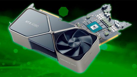
The Nvidia Ada architecture brought a host of new features and astonishing levels of performance to the PC when it launched last year, and in this feature we’re going to unpick the inner workings of silicon wizardry behind the latest Nvidia GeForce gaming GPU range.
As our GeForce RTX 4090 review and GeForce RTX 4080 review have shown, the latest Nvidia GeForce GPU models are monstrously powerful, even if their prices aren’t particularly wallet-friendly. Using these two GPUs as examples, much of that increase in processing capability comes from the AD102 and AD103 GPUs that sit at the heart of these cards.
By switching from the larger Samsung 8N manufacturing process used in RTX 3000-series GPUs, such as the Nvidia GeForce RTX 3070 Ti, to a brand-new TSMC 4N process, Nvidia has been able to squeeze more of all the building blocks that make up a GPU into the die without it becoming unwieldy.
The numbers involved in this change are more than a little mind-boggling. The AD102 GPU packs in a ludicrous total of 76 billion transistors and 18,432 CUDA cores. That’s more than double the 28 billion transistors and nearly double the 10,752 CUDA cores of the GA102 GPU used in the GeForce RTX 3090 Ti. The AD102 isn’t subtle.
The new process also brings improvements in performance thanks to the ability to run at increased clock speeds. Where the GeForce RTX 3090 ran at a base clock of 1395MHz with a boost clock of 1695MHz, and the RTX 3090 Ti increased these figures to a 1670MHz base clock and 1890MHz boost clock, the RTX 4090 runs at a 2235MHz base clock and 2520MHz boost clock.
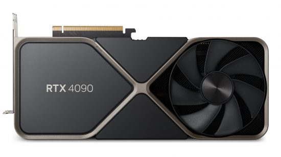
The RTX 4080, with its 9,728 CUDA cores ticks along slightly slower at a 2205MHz base clock and 2,505MHz boost clock, but those are still big leaps over the 1440MHz base clock and 1710MHz boost clock of the GeForce RTX 3080.
Originally there were three cards in the launch line-up – the RTX 4090, RTX 4080 16GB and RTX 4080 12GB. However, because of a strong negative reaction to the significantly lower overall specs of the RTX 4080 12GB compared to the RTX 4080 16GB, it was ‘unlaunched’ and rebranded as the Nvidia GeForce RTX 4070 Ti.
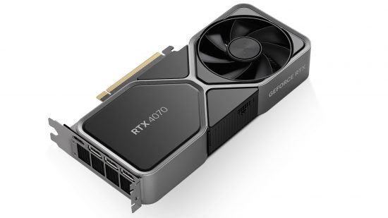
These cards have 4GB less VRAM than the GeForce RTX 4080, as well as far fewer CUDA cores (7,680) and a 192-bits wide memory interface compared with the 256-bits wide interface on the 16GB version. Since then, we’ve also been given the Nvidia GeForce RTX 4070, which has 5,888 CUDA cores, and the Nvidia GeForce RTX 4060 Ti, which has 4,352 CUDA cores. Recently, Nvidia also launched the GeForce RTX 4060, which uses the AD107 GPU and has 3,072 CUDA cores.
As well as these ‘more of everything in a smaller space’ changes, the Ada architecture also brings several other under-the-bonnet tweaks compared with the Ampere architecture that preceded it. The most prominent of these is improved ray-tracing performance, thanks to the development of a new RT core, and improved matrix operation performance thanks to a new Tensor core.
New software features are also being launched along with the new hardware. DLSS 3, the latest version of the company’s upscaling technology, introduces optical flow acceleration, which inserts entirely new extra frames in between traditionally rendered frames, resulting in big frame rate increases for minimal processing outlay.
Meanwhile, shader execution reordering enables developers to more efficiently order the execution of ray-tracing calculations, providing up to a 2x performance in ray-tracing shader throughput.
Nvidia Ada manufacturing process
Although the microarchitecture of a chip can be considered separate from the manufacturing process used to produce it, in practice architectures are generally optimized to work with a specific manufacturing process.
As such, the move from using Samsung’s 8N manufacturing process for its Ampere GPUs to TSMC’s 4N process for its Ada GPUs is an integral part of the difference between Nvidia’s two most recent architectures, and it’s the natural place to start when talking about such an enormously complicated GPU.
TSMC’s 4N process is a refined version of its 5N process – both are still classed as 5nm component-size processes, but the 4N process has a slightly higher density. While 5N has a density of around 138 million transistors per mm² (MTr/mm²), 4N has a density of 146MTr/mm². The 4N process also brings up to an 11 percent increase in potential clock speed over 5N. Those density figures compare to a mere 45MTr/mm² for the Samsung 8N (8nm) process used to make Nvidia’s Ampere GPUs.
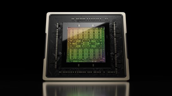
As a result of this huge increase in transistor density, the die size of the AD102 is ‘only’ 608.5mm² compared to the 628.4mm² of the GA102, which itself already saw a significant drop in size compared with the TU102 GPU (used in the top-tier RTX 2000-series GPUs and manufactured using a 12nm process). That chip had a whopping area of 754mm² despite packing in only 18.6 billion transistors.
For context, the AMD Radeon RX 6950 XT uses a GPU called the Navi 21 (based on the AMD RDNA2 architecture), which measures 520mm² and incorporates 27 billion transistors. Compared to the 28 billion transistors in the 628.4mm² die of the GA102, this translates to a slightly higher transistor density, which comes courtesy of AMD’s use of TSMC’s 7nm process for this last-gen GPU, which has a density of 51.5MTr/mm² compared to the 45MTr/mm² of Samsung’s 8N process.
Meanwhile, AMD’s latest RNDA 3 GPUs, such as the AMD Radeon RX 7900 XT use a chiplet design where multiple smaller dies are combined. The main GPU functions remain on a single die, rather than being split up into multiple chips, and instead, it’s the large caches and memory interface elements that have been offset onto other dies.
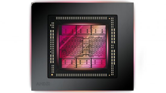
The upshot is that the main Graphics Compute Die (GCD) of the AMD Radeon RX 7900 XTX measures just 300mm², but it’s joined by six 37mm² Memory Cache Dies (MCDs). Although the size difference between the GCD and Nvidia’s AD102 is huge, suggesting there’s a lot of sense to this chiplet approach, AMD’s design does also use fewer transistors in total. The total transistor count of one GCD and six MCDs is 58 billion, compared to the 76 billion of AD102.
AMD’s GCD is produced on TSMC’s 5N process, rather than its latest 4N process, while the MCDs will use TSMC’s even older, cheaper and slightly larger 6nm process. In theory, this production method should result in cheaper overall production costs, due to the higher yields associated with smaller dies, but will come at the expense of slightly lower clock speeds and power efficiency as both processes are larger than the ones used to make Nvidia’s latest GPUs.
Back to Ada Lovelace’s new process and, as already highlighted, it brings with it big leaps in clock speed over the older Samsung process and improvements to power efficiency. Those base and boost clock improvements from the RTX 3090 to the RTX 4090 highlighted earlier amount to 60 percent and 49 percent upticks respectively. Those are big leaps by any measure.
Meanwhile, power efficiency has taken a huge step forward, with Nvidia claiming the RTX 4090 will deliver double the performance of the RTX 3090 when running at the same power level. This is a claim we saw borne out in our testing, with the RTX 4090 using significantly less power than the RTX 3090 and RTX 3090 Ti when not maxing out the card’s performance.
Of course, not content to just hit that same power level as before, Nvidia has pushed the RTX 4090 beyond the same power envelope as the RTX 3090, so that it boasts a 450W total board power compared to the RTX 3090’s 350W. Again, this was shown in our testing when we really pushed the card hard at 4K with ray tracing – the RTX 4090’s total system power draw leaped from 535W when running at 2,560 x 1,440 resolution to 619W when running at 4K.
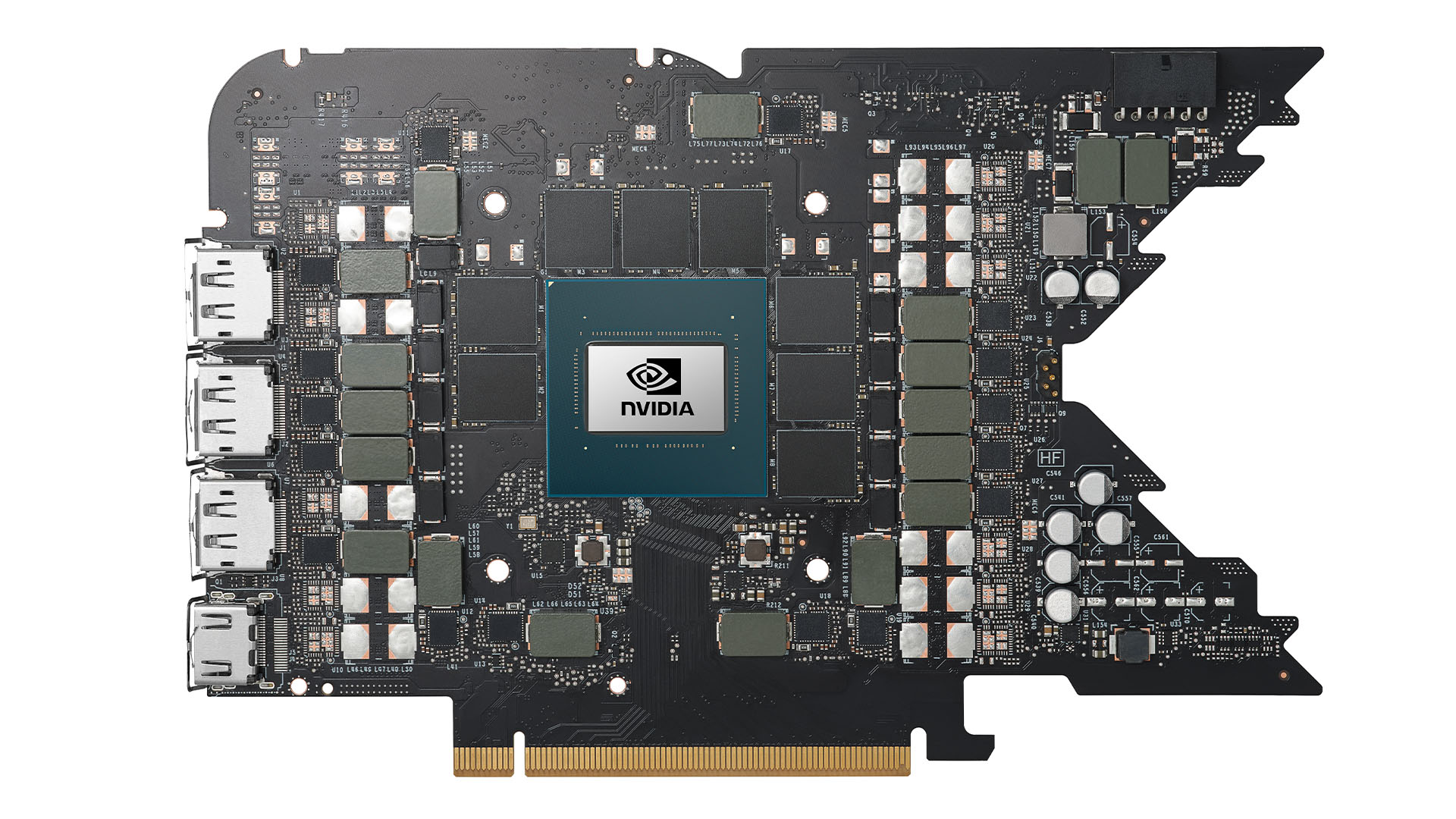
In order to accommodate these power requirements, and to neaten up the cabling, Nvidia has used the new 12VHPWR 16-pin power from the ATX 3 spec to accommodate the power delivery. However, some people have experienced these connectors melting under the load of the card if they’re not installed and handled carefully – some versions of these connectors have soldered joints that can crack if the cable is bent.
In comparison, AMD’s RX 7900 XTX has a still very high total board power of 355W, but the cards use two conventional 8-pin PCIe power supply plugs, rather than a proprietary new connector.
The power draw situation isn’t so dramatic as you start moving down the stack of Ada graphics cards, with the RTX 4080 16GB already dropping to a 320W total board power and the RTX 4070 Ti having just a 285W total board power.
Nvidia Ada building blocks
While the change in manufacturing process is a huge part of the overall performance and efficiency improvements of the RTX 4000-series GPU line-up, Nvidia has also tweaked the underlying architecture. Many of the core building blocks are very similar to the company’s previous Ampere architecture but there are several tweaks throughout.
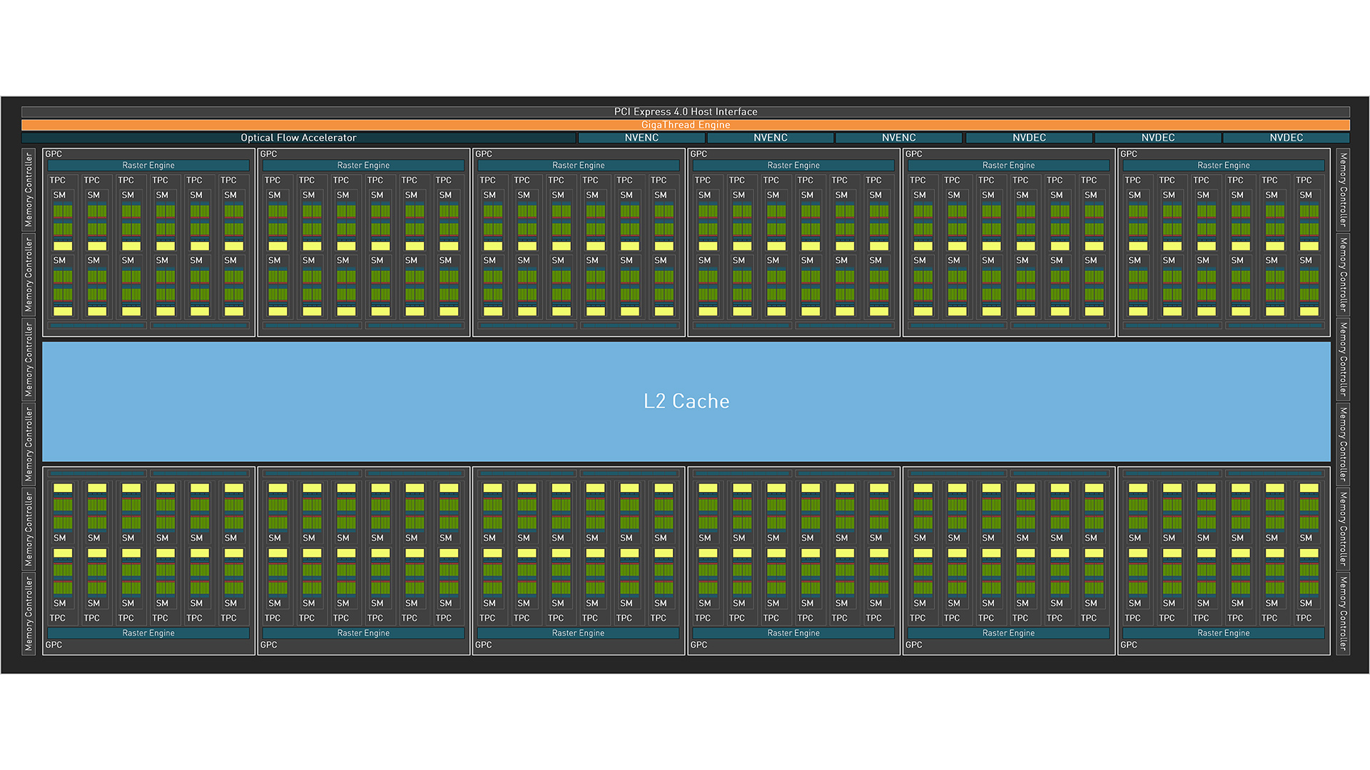
If we look at the block diagram of the AD102 GPU that powers the RTX 4090 and RTX 4080, we can see that it’s very similar to the GA102 GPU that preceded it, just with more of everything. Around a central core of L2 cache are arranged 12 graphics processing clusters (GPCs), each of which contain six texture processing clusters (TPCs) and an accompanying raster engine.
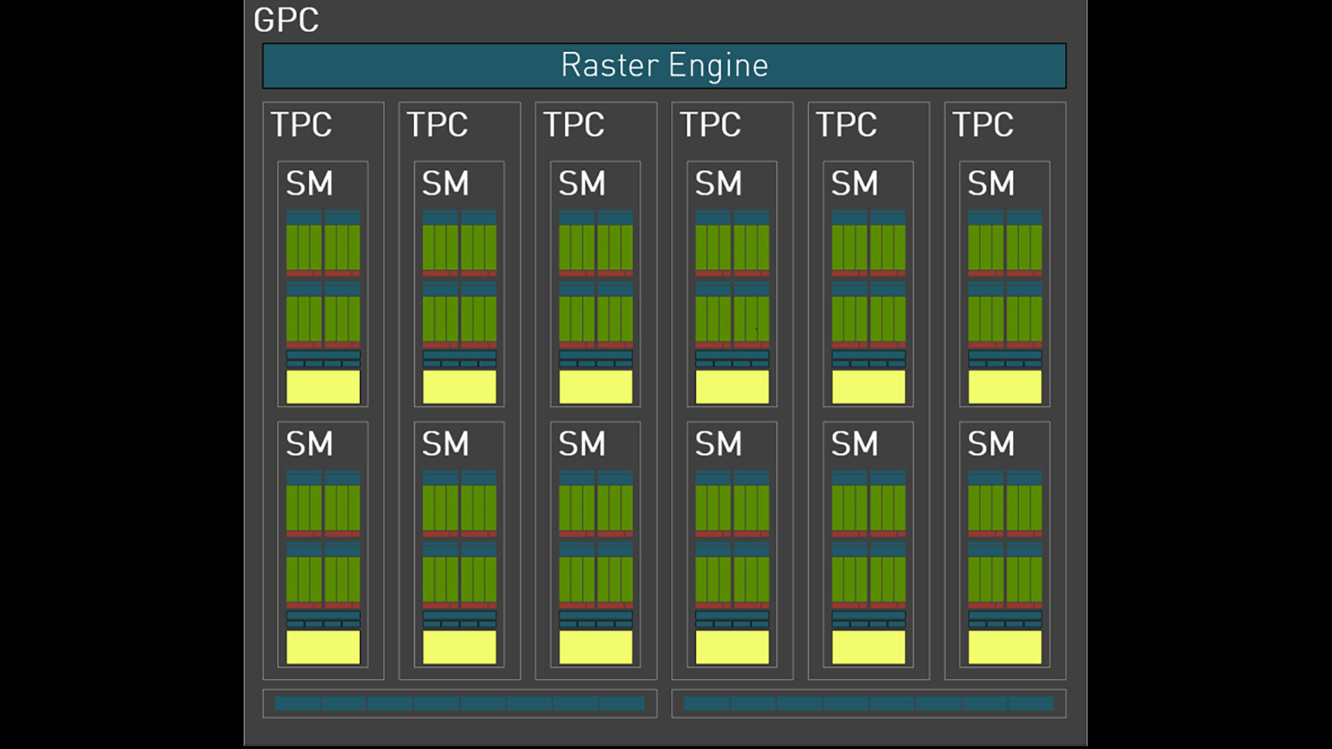
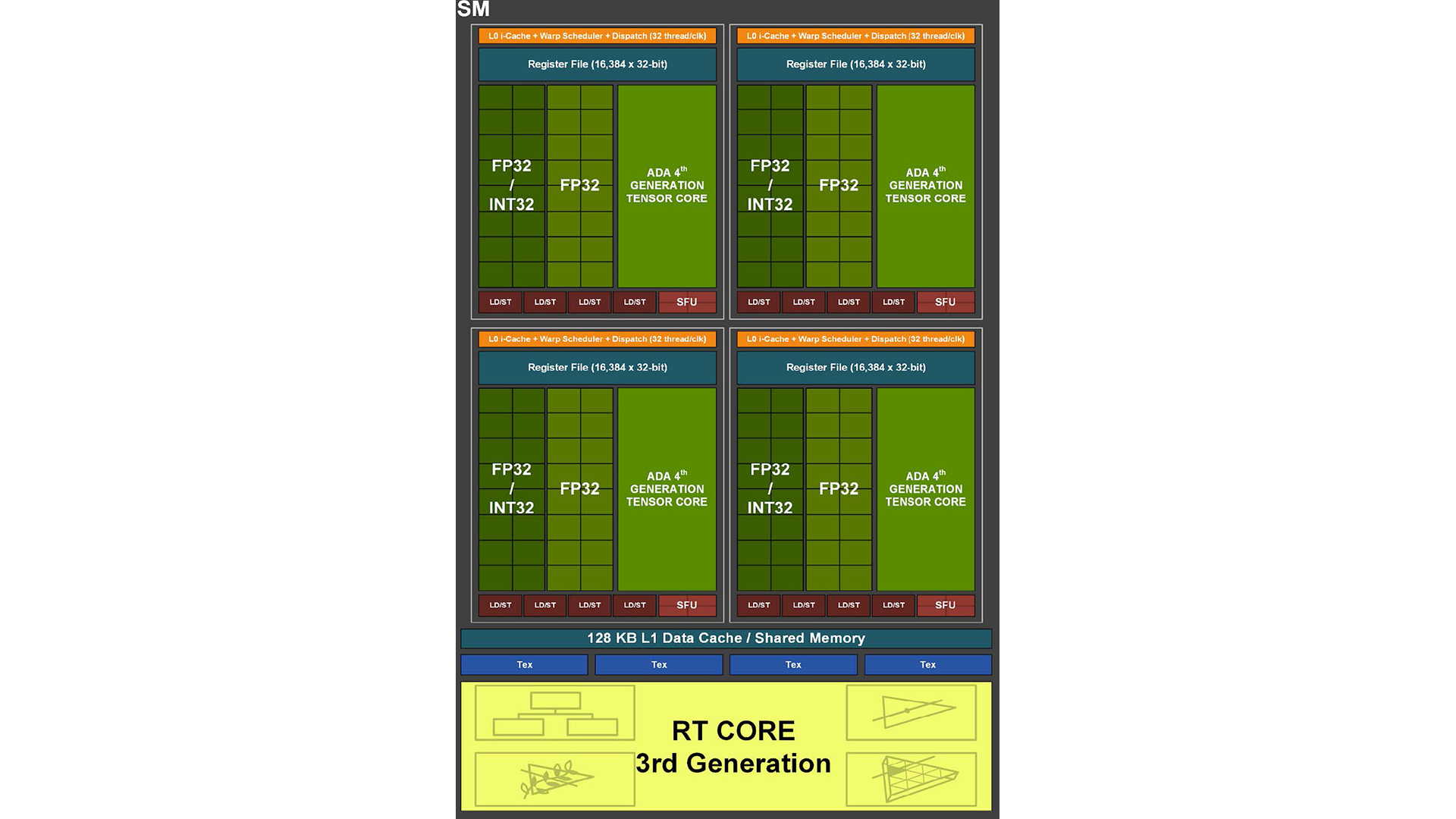
In turn, each of these TPCs houses one Polymorph engine (for tessellation and other geometry shading functions) and two streaming multiprocessor (SM) blocks. The latter are arrangements of 128 CUDA cores separated into four further sub-blocks, four texture units and four Tensor cores, joined by one RT core per SM.
CUDA cores are the heart of Nvidia’s GPUs. They come in two different types, with some able to process just 32-bit floating point (FP32) operations and some able to process either one FP32 operation or an integer (INT) operation per clock cycle.
Combined into two blocks of 16 of each type, these blocks of 32 CUDA cores are delivered tasks in waves, with each block of cores performing the same function on multiple sets of data at once. This enables the efficient parallel processing that’s the central tenet of good GPU design.
Each block of 32 CUDA cores is also joined by one Tensor core for performing specialized matrix multiply and accumulate operations – more on this later – along with four load/store units for memory loading and storing operations, and a block of four special function units for performing operations such as sin, cosine, reciprocal and square root. There’s also a 16KB register file, L0 instruction cache and the warp scheduler, which distributes the waves of operations to the CUDA cores.
If you zoom back out to look at the whole die block diagram you can see that atop – from a block diagram perspective, not necessarily a physical arrangement perspective – this arrangement of SMs, TPCs and GPCs is the PCIe 4 interface, the new Optical Flow Accelerator, the NVENC video encoder blocks and the GigaThread Engine. The latter manages the overall schedule of work for the whole GPU.
Compare this arrangement with the block diagram of the Ampere architecture’s GA102 GPU, and we can see that the older architecture had this same arrangement of building blocks. A total of 128 CUDA cores, four Tensor cores and one RT core are combined to form one SM, then two SMs, then add one RT core and a Polymorph engine to form each TPC. Twelve TPCs then go on to form each GPC when combined with a raster engine block.
The most obvious difference between these two chips, then, is that the new AD102 chip houses 12 GPCs but the GA102 contains only seven. As a result, while the AD102 contains 18,432 CUDA cores, 144 RT cores, 576 Tensor cores and 576 texture units, GA102 packs only 10,752 CUDA cores, 84 RT cores, 336 Tensor cores and 336 texture units.
Other obvious differences between the two block diagrams include the size of the L2 cache. This change in block size is indeed reflective of the massive hike in L2 cache that Nvidia has packed into the AD102. Whereas GA102 houses 6,144KB of L2 cache, AD102 has 98,304KB – 16x more.
Nvidia claims this larger cache has benefits across the board, particularly for budget GPUs that have a narrower memory interface than the current Ada lineup, and it’s particularly beneficial for complex operations such as ray tracing. Otherwise, that’s it for key differences that Nvidia has made public, other than the addition of new RT and Tensor cores.
Nvidia Ada ray tracing RT core
The biggest single block change to the Ada architecture, at least from the point of view of benefits to a user, is the addition of a new 3rd-generation RT core. Like previous iterations of its RT cores, the new versions have a Box Intersection Engine for calculating bounding box ray intersections, and a Triangle Intersection Engine for calculating triangle ray intersections. However, this 3rd-generation core also introduces two new blocks – an Opacity Micromap Engine and a Displaced Micro-Mesh Engine.
To recap, bounding box intersections are the first step in calculating how rays interact with a scene. In order to keep processing to a minimum, bounding boxes (or volumes) are created around objects (or parts of objects) within a scene, and a bounding volume hierarchy (BVH) table is generated, which defines the order of bounding volumes in the scene. As a result, there might be one bounding volume for a whole building, which then contains multiple bounding volumes defining rooms and a further volume defining an object within that room.
When calculating the paths of a ray, the algorithm first checks whether any rays intersect the outermost/largest volume. If the ray misses the volume, no more work needs to be done for all the objects or volumes within that volume. However, if the ray does intersect with the first bounding volume then the ray moves further into the BVH, checking the next intersections with these smaller bounding volumes.
Once the full BVH has been traversed, the next stage of the process is calculating the intersection of the ray with the triangles that make up the objects in each intersected volume. With Ada, the bounding box engine hasn’t seen a boost in performance but the triangle intersection engine has been improved, with the new Ada engine boasting a doubling in throughput compared to Ampere.
As for those two new blocks, the first of these deals with a specific problem to do with using transparent textures for creating detail on flat surfaces in on-screen objects. Rather than forming complex objects, such as chain-link fences or the hundreds of leaves on a tree out of complex geometry, game engines use flat images (textures) with transparent sections (the gaps in the fence or between leaves) and paste these onto simple flat objects.
That works fine for normal rasterization tasks, but when you introduce ray tracing, and you have to calculate how a ray interacts with all the fine transparent details of that texture, you end up throwing off the efficiency of the highly optimized triangle intersection accelerator.
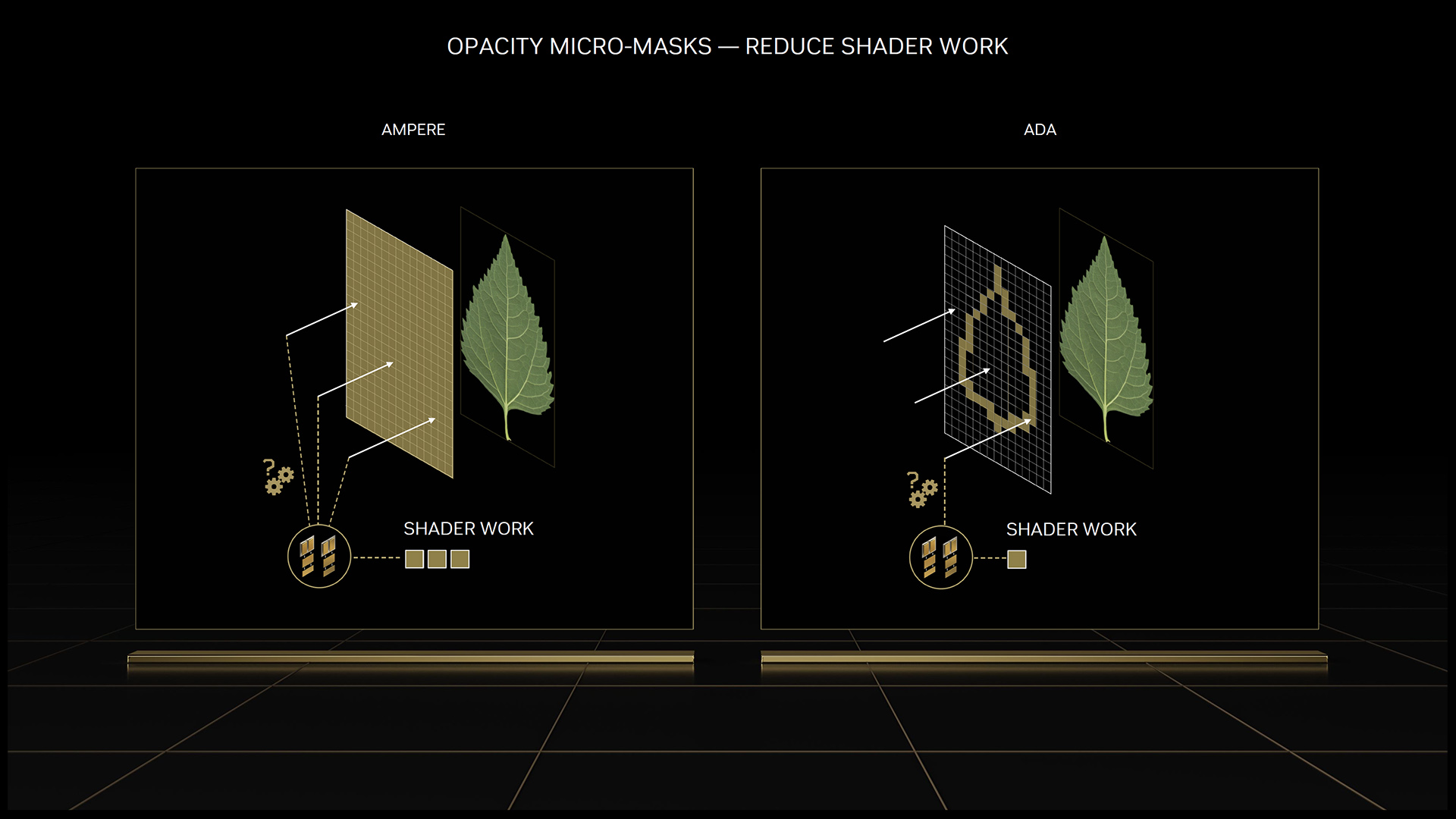
The Opacity Micromap Engine, then, takes these textures and forms an opacity micromap from them, which defines the texture as a grid of tiny triangles, each with an opacity state of opaque, transparent or unknown (the latter is for triangles that are neither fully transparent or opaque). If the triangle is transparent, the ray intersection can be ignored. If it’s opaque, a hit is recorded and returned. Finally, if it’s unknown, control is returned to the SM for further shader work to be undertaken.
The key to this micromap is that it allows the triangle intersection engine to treat most of the transparent texture in the same manner it treats other solid-object triangles, so it can rattle through the calculations quickly. Without this ability, further shader operations are required that interrupt this efficient process. Nvidia says it has observed up to ‘a doubling of scene traversal performance in applications with alpha-tested geometry’, but points out that the performance advantage is very scene dependent.
As for the Micro-Mesh engine, this deals with the complication that arises from using tessellation. This is where a simple version of a 3D object is used for some parts of the graphics pipeline, and then extra triangles are added to the object later to add more detail, using techniques such as displacement mapping.
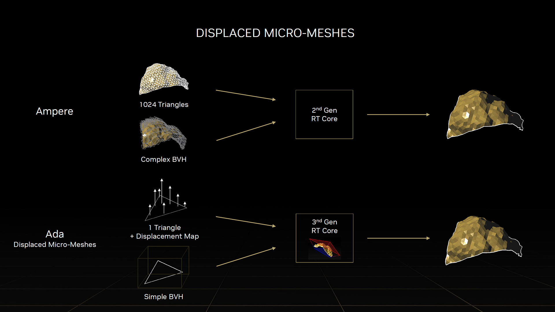
These extra triangles greatly increase the complication of the bounding volume hierarchy (BVH), so the micro-mesh engine recognizes where tessellation has occurred and uses the simpler form of the model to calculate a baseline of how rays interact with it. It then moves on to using the full complex model for the next stages of rendering the scene.
The upshot of the Micro-Mesh engine is significantly faster generation of the BVH and a significant reduction in the complexity and size of the BVH. In three examples Nvidia has provided, the BVH generation was on average 10x faster and 11x smaller than without the Micro-Mesh engine.
The upshot of these ray-tracing improvements is that Nvidia extends its already considerable lead over AMD when it comes to ray-tracing performance. The AMD RDNA 3 architecture boasts a 1.5-1.7x improvement in ray-tracing performance over RDNA 2, but that’s only enough to close the gap between RDNA 3 and Nvidia’s older Ampere architecture.
Nvidia Ada Tensor core
Another area where Nvidia has historically held a distinct advantage over AMD is in having GPU hardware for matrix multiply and accumulate operations, which are commonly used in AI and high-performance computing applications.
The Tensor cores in the company’s existing architectures are dedicated to these functions and hold a huge performance advantage over performing the same functions using the general-purpose compute units (CUDA cores) of the GPU.
AMD, in contrast, does have such dedicated cores in its latest RDNA 3 architecture, with two new AI accelerator cores in each compute unit, but it doesn’t currently have any gaming features such as DLSS that can take advantage of them.
Back to Nvidia, the new Tensor cores in the Ada architecture deliver more than double the FP16, BF16, TF32, INT8, and INT4 performance (measured in the distinctly non-standard unit of Tensor TeraFLOPS) of the previous Ampere architecture. The company’s Hopper FP8 Transformer Engine for accelerating the training of AI has also been added, delivering over 1.3 PetaFLOPS of tensor processing in the RTX 4090.
The significance of this in games that don’t support DLSS is basically non-existent, but Nvidia’s new DLSS 3 AI frame generation tech relies heavily on the latest Tensor core design to make its calculations as quickly as possible.
What is Shader Execution Reordering?
Two of the biggest new features to arrive with the Ada Lovelace architecture are software features that Nvidia has provided for developers. The first of these is Shader Execution Reordering (SER), which looks to solve the problem of GPUs being best suited to running a single function across multiple pieces of data, which causes problems when you introduce ray-tracing workloads, which inherently result in unordered, jumbled up workloads.
The reason for this disorder is that ray tracing works by calculating the paths of rays of light interacting with the surfaces of objects in a scene, and while the first stream of rays and their surface collisions can be calculated in parallel batches – because they all have the same starting point and direction, so they tend to meet the same surface in order – for subsequent bounces of each ray, they could all be going off in completely different directions, depending on the surface with which they interact.
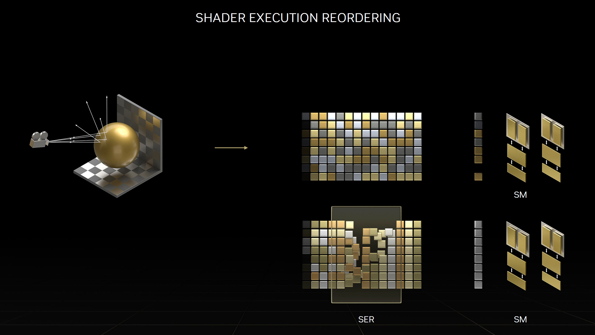
SER, then, allows a developer to step in and, instead of having the second ray bounce calculations performed in the same order as the first bounces – and as a result, potentially be invoking all manner of different shader operations, depending on the secondary surface with which the ray is interacting – they can reorder the second bounce calculations to be performed in clusters, based on the second surface the rays are hitting.
This then means the GPU can more efficiently invoke the shader operations for that surface on several of the rays at once, before moving onto a different shader operation for the next surface and its set of ray interactions.
According to Nvidia’s figures, SER can provide up to a 2x performance improvement for ray-tracing shaders with high levels of ray divergence. As a real-world example, it says Cyberpunk 2077 can benefit to the tune of up to 44 percent faster performance when running with the game’s new Overdrive mode.

DLSS 3 and Optical Flow Acceleration
The final major piece of the Ada puzzle is the introduction of deep learning super sampling 3 (DLSS 3), which … is not a good name for this new technology.
You see, DLSS 3 is not a super-sampling technique (deep learning or otherwise) for upscaling lower-resolution game output to look better on higher-resolution screens. Instead, it uses similar AI-derived image generation techniques to DLSS 2 but to create entirely new frames. It’s so unrelated to DLSS 1 and 2 that you can even enable DLSS 3 without lowering the output resolution of your game – no upscaling will be happening at all, just extra frame generation.
The technology uses motion vectors from the game (a measure of how objects and the view were moving when the current frame was generated), and the previous output frame to generate a guess at a new version of that frame. So, rather than increasing your game’s frame rate by reducing the initial workload of the graphics card, and upscaling the output, DLSS 3 instead keeps your graphics card working at full pelt to generate the best initial image quality, but then provides a smoother-looking experience by upping the frame rate with ‘fake’ frames.
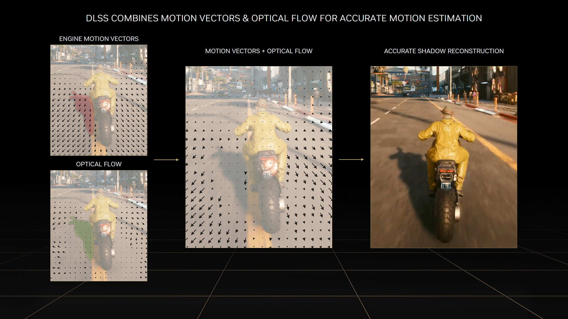
It’s an interesting twist on the idea of AI frame generation and the performance uplift is striking. In our own testing with the GeForce RTX 4090, we saw Cyberpunk 2077 leap from a 68fps average at the Medium ray-tracing preset with DLSS 2 on its Balanced setting, to 118fps with DLSS 3.
That compares to only 46fps on the RTX 3090 Ti using the Medium ray-tracing preset and DLSS 2 in Balanced mode. Even the GeForce RTX 4070 can cope well with running Cyberpunk 2077 in its latest Overdrive mode if you enable DLSS 3, averaging 86fps at 1,920 x 1,080 with DLSS 3, compared with 49fps without it.
The downside to DLSS 3 is that, just as with previous versions of DLSS, the performance uplift comes with some image quality compromises. Fast motion can throw off the frame generation predictions, creating blurred details and halo effects around moving objects.
Drastic changes in image, such as your view moving from out behind a wall, can result in completely garbled, made-up images that are half wall and half the view beyond. In testing, we saw occasional artifacts in our custom benchmark, based on a 60-second repeatable drive around Night City, including a line consistently appearing in a wall at the start.
A key positive with this technology, though, is that while these effects are more prevalent in fasting-moving game types, such as first-person shooters or racing games, they become inherently less noticeable as the frame rate climbs.
That’s because, unlike DLSS 2 where every frame is affected by the upscaling, with DLSS 3 you can potentially still see normal, unaffected frames (assuming you run DLSS 3 at native resolution) interspersed with what can sometimes be iffy-looking fake frames, so as the frame rate increases, the time that each ‘bad’ frame is shown decreases.
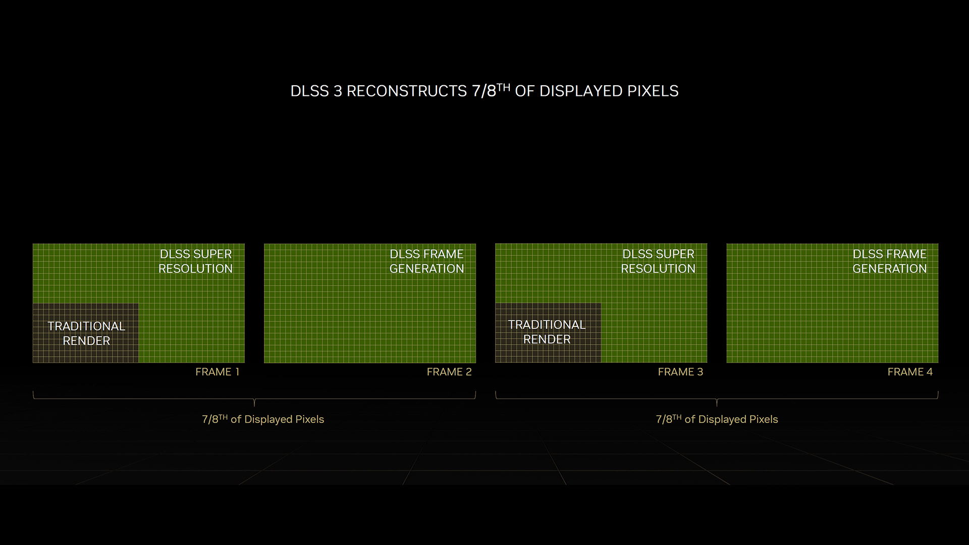
So, if your game’s running at 30fps, each generated frame is shown for a very noticeable 33ms, whereas at 120fps, you’re only seeing a ‘bad’ frame for 8ms.
As a result, you still get the benefit of a smoother frame rate to help you better judge your aim, or the braking point for a corner, for instance, without constantly being thrown by incorrect image artifacts.
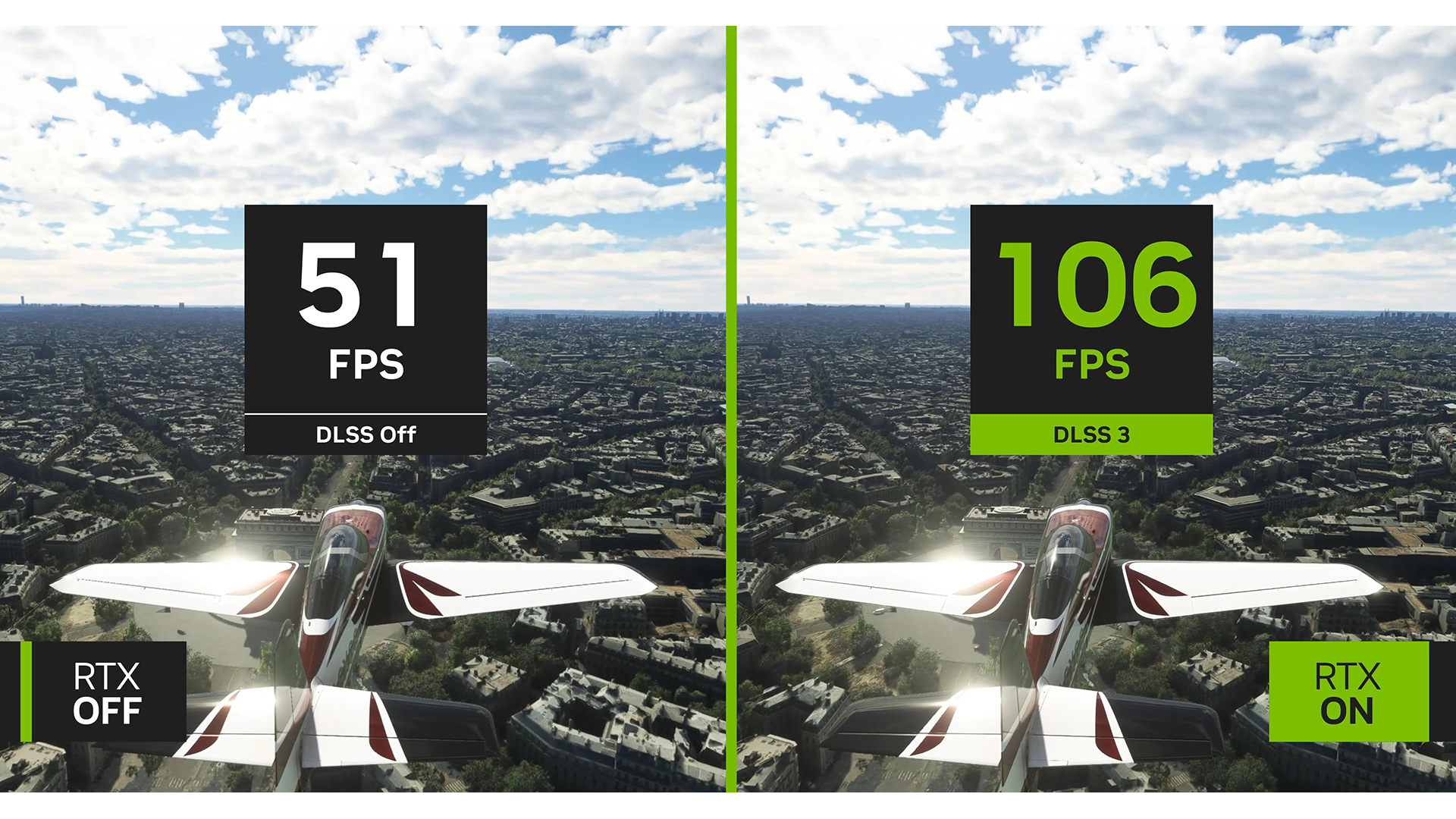
DLSS 3 can also reduce the load on your CPU when you’re playing games with high frame rates – as the CPU’s essentially not doing anything for half the frames. As such, there’s potential for some gamers to find a better overall performance balance by turning on DLSS 3, if their CPU is proving a bottleneck. Games such as Microsoft Flight Simulator are cited as examples where a fast, smooth frame rate are required along with a lot of CPU work.
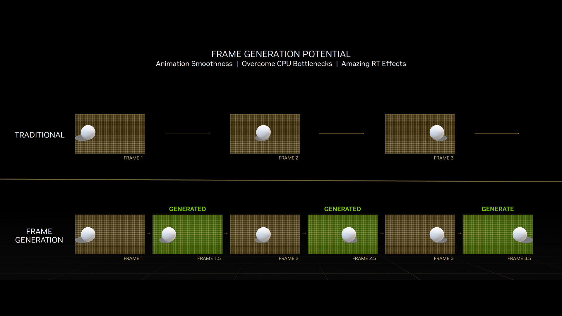
While DLSS 3 is mostly a software system, like previous DLSS implementations, it takes advantage of Nvidia’s dedicated Optical Flow Accelerator engine, which is essentially a refined version of the optical flow accelerators used to encode and decode video. Despite these being present on previous RTX cards, though, for now DLSS 3 is being restricted to only working on RTX 4000-series cards. Here’s hoping Nvidia adds support for older cards too in the future.
We hope you’ve enjoyed taking a deep dive into the Nvidia Ada Lovelace GPU architecture with us. If you’re on the lookout for a new graphics card, then check out our full guide to the best graphics card, where we list several options at a range of prices. If you already own an Ada card, then take a look at our full guide on how to water-cool GeForce RTX 4080 and 4090 graphics cards.
