AMD’s new RDNA 2 graphics architecture has been a long time coming, the driving force behind the long-awaited and much anticipated ‘Big Navi’ discrete GPUs. Already deemed worthy by Sony and Microsoft for use in both the PlayStation 5 and Xbox Series X, the launch of the RX 6000-series graphics cards now presents RDNA 2 to the most discerning client of all: the PC gamer.
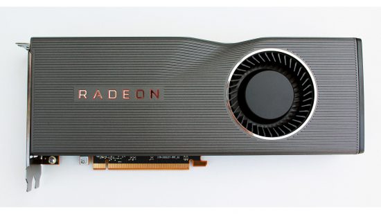
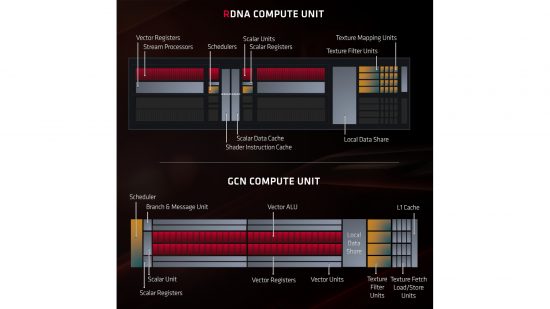
RDNA originally launched last year, following a full eight years of iterative updates to Graphics Core Next (GCN) – the AMD architecture launched for PC in 2011 via the Radeon HD 7970. As a truly new architecture, then, RDNA was a welcome change in 2019, making its PC debut in the 251mm² Navi 10 GPU. In its full implementation comprising 40 Compute Units (CUs), this GPU powers the RX 5700 XT; at launch, it easily outperformed the GCN-based Vega 64 while consuming less power and using 24 fewer CUs.
With a redesigned CU, a new multi-level cache hierarchy, and a streamlined pipeline, Navi was a healthy step forwards in performance. It also injected AMD graphics cards with a desperately needed boost to efficiency, or performance per watt (PPW). In fact, the PPW increase was around 50 per cent, largely assisted by the move from 14nm to 7nm manufacturing.
However, Navi’s launch was underwhelming for those hoping for a takedown of Nvidia akin to Ryzen’s impact on Intel CPUs. The £380 launch price certainly humbled Nvidia into some price cuts for mid-range RTX 20 Series cards, but it also told consumers that AMD still had no stake at the top of the GPU market, while the RTX 2080, RTX 2080 Super and RTX 2080 Ti were left unphased despite having launched almost a year before.
Worse still, Nvidia maintained a small edge in efficiency, even though Turing was manufactured on 12nm, and RDNA 1 noticeably had no answer to Nvidia’s support for real-time ray tracing, which was (finally) gaining some traction and appearing in games.
With the first Navi launch, AMD had stronger products but still had significant ground to reclaim in three key areas: performance, efficiency and features. For those hoping for better competition across the entire GPU market, hope quickly shifted to Big Navi. To say there’s been an appetite for RDNA 2 and Big Navi among PC gamers would be an understatement.
RDNA 2 overview
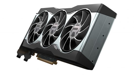
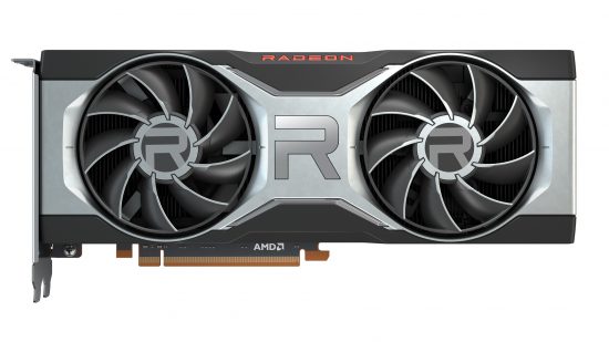
All of which brings us to today. By now, Nvidia has extended its lead over AMD even further with Ampere and the RTX 30 Series. Nevertheless, AMD has finally brought the fight to Nvidia where it was needed most – at the top. The RX 6000 series currently comprises three cards, with the Radeon RX 6800 and RX 6800 XT priced at £530 and £680 respectively, and the forthcoming Radeon RX 6900 XT waiting in the wings to take on the RTX 3090.
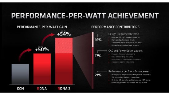
Remember those three key areas? With the RX 6000 series, AMD claims it can deliver up to double the frame rate of the RX 5700 XT and up to 54 per cent more PPW, ticking off the performance and efficiency criteria. As you can see in the results on p20, it’s not far off. As for features, the RX 6000 series graphics cards come with full, hardware-level support for DirectX 12 Ultimate, including dedicated logic for real-time ray tracing.
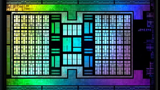
Making all this possible is the Navi 21 GPU, which powers the RX 6900 XT, RX 6800 XT and RX 6800. This 26.8 billion-transistor GPU measures 519.8mm² and houses 80 Compute Units, essentially doubling in size over Navi 10 – Big Navi definitely lives up to its name. Indeed, it’s worth reiterating just what Big Navi represents. AMD simply didn’t release a ‘big’ GPU based on its first RDNA architecture. Big Navi not only brings all the improvements of RDNA 2 with it, but it’s also is simply the first ‘big’ GPU AMD has released in some time.
The inherent parallelism of GPU computing means that adding more Compute Units in this way (going wider) is a guaranteed way to boost performance. The other way to ensure more frames per second is to go faster with a clock speed increase. With boost clocks well north of 2GHz on all three cards, Big Navi has achieved this as well.
The cost of going wider and faster is, of course, power draw. One ‘easy’ way to save power is to transition to a more efficient node (just as we saw with the move from GCN to RDNA), but AMD is sticking to the same TSMC 7nm process with these GPUs. Nevertheless, where the RX 5700 XT had 40 CUs and a boost clock of 1905MHz, resulting in a total board power of 225W, the RX 6900 XT has fully double the CU count and an 18 per cent higher boost clock, yet the total board power has only increased to 300W.
This figure also compares favourably with the competition, with the GeForce RTX 3080 and RTX 3090 hitting 320W and 350W respectively. As you’ll see in our results on p20-21, our system did indeed draw 29W less at peak load with the Radeon RX 6800 XT than with the GeForce RTX 3080.
The specifics of AMD’s efforts in crafting RDNA 2 for Big Navi are what we’ll be exploring in this feature. The inimitable CPC reviews team will of course delve into quite how well the GPU performs in its different configurations. In this feature, we’re looking more closely at how it performs. Let’s start by familiarising ourselves with how the GPU is configured.
Navi 21
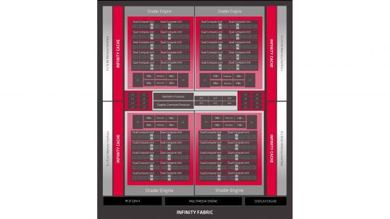
With one key exception, the high-level structure of Big Navi hasn’t changed all that much. The Graphics Command Processor receives the CPU’s API commands via the PCI-E 4 bus, and in turn it has one command stream for each type of shader program (one for vertex shaders, one for pixel shaders and so on). We also again have four Asynchronous Compute Engines, each with its own independent command stream, which manage compute shaders. The scheduling logic means graphics commands can be entirely suspended when a latency-sensitive, high-priority compute task needs to be carried out.
The majority of work is again distributed between the Shader Engines, which house all of the programmable compute resources. Meanwhile, the Geometry Processor lives up to its name, managing the fixed-function pipeline and assisting with tasks such as tessellation and vertex assembly.
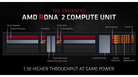
Each of the four Shader Engines of this GPU contains ten Dual Compute Units, which AMD describes as ‘the essence of the RDNA architecture’. Each of these has four of the 32-wide SIMDs (128 stream processors) introduced with RDNA last year, as well as eight texture units and two scalar units. In its full implementation, as used in the RX 6900 XT, Navi 21 is rocking 5,120 stream processors, 320 texture units and 160 scalar units. These counts are reduced in line with the Compute Units, with the RX 6800 XT having 72 active CUs and the RX 6800 having 60.
Navi 22
Since the original Navi 21 launch, AMD has also released the Radeon RX 6700 XT, which is based on a smaller GPU called Navi 22 and based on the same RDNA2 architecture. Te Navi 22 die measures just 336mm², compared with the 519mm² Radeon RX 6800-series GPUs. This little die contains 17.2 billion transistors and of AMD’s RDNA2 40 compute units, and the whole chip is fully enabled on the Radeon RX 6700 XT.
As with Nvidia’s GeForce RTX 3060, the Radeon RX 6700 XT also has 12GB of GDDR6 memory attached to a 192-bit memory interface. On paper this gives the card a total memory bandwidth 384GB/sec in conjunction with the 2GHz (16GHz effective) memory. However, AMD claims that the chip’s 96MB of on-die Infinity Cache will significantly reduce latency here, as the GPU will have quick access to a large pool of memory that’s much faster than the GDDR6 memory.
Each of the chip’s 40 compute units contains a dedicated Ray Accelerator for ray tracing in games, along with 64 stream processors, making for a total of 2,560. What’s more, the GPU has a game clock of 2424MHz – as a point of comparison, the mighty Radeon RX 6900 XT has a 2015MHz game clock.
It’s for this reason that AMD’s quoted board power of 230W isn’t far off the 250W for the Radeon RX 6800 – the Radeon 6700 XT’s small chip might have less parallel processing power than the Navi 21 chip in the Radeon RX 6800, but the high clock speed pushes up the power draw.
Infinity Cache
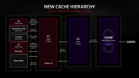
Aside from the overarching increase in CU count per Shader Engine in RDNA 2 vs RDNA, from a block diagram perspective, the single biggest difference is the introduction of a very large cache block, dubbed Infinity Cache. This 128MB cache is shared across the entire GPU, and it provides a massive pool of relatively fast-to-access data, which saves the GPU from having to resort to querying the much slower pool of GDDR6 memory.
To put Infinity Cache into perspective, the rest of the GPU’s cache structure consists of a selection of 16KB and 32Kb L0 caches that are available to each CU, then there’s a 128KB L1 cache shared across each Shader Engine. A larger 4MB block of L2 cache is then shared across the whole GPU. For RDNA that was it – 4MB of L2 cache then straight on to GDDR6. As you can see, the introduction of a massive new block of 128MB of L3 cache is quite something.
The advantages of an extra level of cache are fairly obvious, as any data store that’s kept on the GPU die is (generally) inherently much faster than one kept on a separate chip. In an ideal world, the full whack of up to 16GB of memory that comes attached to modern graphics cards would be built right into the GPU.
However, this is neither cost-effective nor practical, as the chips would be enormous and thus expensive and difficult to manufacturer. Indeed, even the addition of a 128MB cache would, according to AMD, be impractical using conventional GPU L2 cache technology that’s optimised for the very high bandwidth demands of a GPU.
To get around the problem of wanting to introduce a very large extra layer of cache without the associated problems, AMD turned to the cache designs it developed for its EPYC CPUs. This type of cache is four times denser than AMD’s existing L2 GPU cache while remaining power-efficient.
The downside is relatively slow performance for a cache. Infinity Cache is accessed via the 16 x 64-byte channels of Infinity Fabric running at 1.94GHz, giving you a total bandwidth of 1.99TB/sec. That’s ‘only’ around four times the 512GB/sec of GDDR6 memory bandwidth you get via the Radeon RX 6800’s 256-bit memory interface with 16GHz (effective) memory.
Putting some further numbers to that claim, the addition of Infinity Cache results in a 34 per cent reduction in effective average memory latency, providing a massive potential uptick in performance.
Along with performance gains, the greater utilisation of on-board cache instead of GDDR6 memory has power consumption benefits too. Where Infinity Cache access uses 1.3pJ of energy, GDDR6 access uses 7-8pJ. With the average number of cache hits rising by up to 58 per cent, thanks to the addition of Infinity Cache, that’s a huge reduction in GDDDR6 accesses and a significant reduction in total board power consumption.
This reduction in the number of overall GDDR6 memory accesses also enables AMD to operate Navi 21 with a relatively narrow 256-bit memory interface, which has its own power-saving benefits. In comparison, while Nvidia’s Ampere-based RTX 3070 also uses a 256-bit interface, the RTX 3090 uses a 384-bit wide memory interface.
Previous AMD GPU designs pushed the boundaries of memory interfaces – most notably with the High Bandwidth Memory (HBM) of the Radeon R9 Fury, which had the memory stacked on the GPU and used a massive 4096-bit wide interface. To see AMD change this strategy so dramatically highlights magnitude of this new cache system.
Further power saving comes from the ability to change the frequency of the Infinity Cache. While dynamic clock speed adjustment isn’t a new concept in processor design, it wasn’t necessarily a given for the Infinity Cache. By allowing the cache to boost up to its 1.94GHz peak speed (for up to 550GB/sec of bandwidth) then drop back down, AMD can further enhance the overall power efficiency of RDNA 2.
RDNA 2 performance-per-clock improvements
Infinity Cache may be the most obvious change to the core number-crunching design of RDNA 2, but it’s by no means the only change. AMD set itself the task of enhancing the clock speed, performance per clock and overall power efficiency of its design, and all three of these factors required a multitude of sometimes large, but often small, incremental changes to achieve a significant overall improvement.
AMD claims that RNDA 2 provides an overall performance per watt (PPW) gain over RDNA of 54 percent. On top of the 50 percent increase RDNA already brought with it over the company’s previous GCN architecture, this is a huge change from the disastrously power-hungry designs AMD was churning out just a couple of years ago.
Looking more closely at each of those three factors, then, we can start with further improvements in the performance-per-clock enhancements RDNA 2 brings, alongside Infinity Cache.
First up is an improved Translation Lookaside Buffer (TLB), which is a component that translates virtual memory addresses to physical ones, and is a crucial part of any processor’s memory and cache management system. The new TLB design now performs physical address translations on L0 misses rather than checks, reducing the overall load on the TLB and its resultant latency. This change benefits all CU vector data requests, resulting in improved overall performance.
Another improvement concerns the render back end (RB) of the GPU’s pipeline. This section is responsible for performing depth, stencil and alpha tests, as well as blending pixels for anti-aliasing. On RDNA, each RB unit (four per Shader Engine) could process four 32-bit pixels per clock. RDNA 2’s RB+ units have upped that to eight 32-bit pixels per clock. The new RB+ section required a complete rework to enable this change, along with adding features to enhance support for DirectX 12’s variable rate shading (VRS) and support for HDR formats.
As well as improving sections of the GPU design in this way, AMD has also improved clock speed and power efficiency across the board through a host of tweaks. A lot of this enhancement is simply down to the company being able to dig deep into the workings of the 7nm process on which the GPU is built.
With AMD’s RDNA and RDNA 2 GPUs, as well as its Zen 2 and 3 CPUs, being built (at least in part) using TSMC’s 7nm process, AMD is already several generations and several architectures into using the process, so it’s gleaned plenty of knowledge about how to get the best from the process. This is undoubtedly similar to the way in which Intel has been able to squeeze ever greater performance from its own 14nm process.
For example, chip design works on multiple levels, in what’s known as cell-based design. For much of the process, a chip designer will be working with higher-level logic structures, such as NAND gates, without any specific knowledge of the underlying process for manufacturing that logic. In this way, AMD’s engineers can largely concentrate on designing the higher-level logic, while its cell partners and manufacturers, such as TSMC, can work on optimising the performance and manufacture of cells.
That’s a very simplified description but it gets the point across. By working more closely with TSMC and its other cell partners, AMD can work on actually improving the performance of the underlying cells, specifying new cell types or at least optimising its logic for those cells.
For instance, AMD can identify common logic patterns that can be replaced by a combined and optimised single logic cell.
AMD has also reduced unnecessary movement of data throughout the GPU with RDNA 2. By minimising data movement between the functional blocks of the GPU, you can save power and then use that power budget to improve performance instead. Similarly, the company has rebalanced the overall graphical pipeline to minimise the amount of extra computation needed between each stage of the pipeline.
Overall dynamic switching power (CAC) consumed by each CU has also been reduced between generations, and ever greater and finer control of clock gating has been implemented. Clock gating is where the clock signal to a part of a processor is disabled, essentially switching off that part of the circuit. By turning off as much of a circuit as possible when it’s not in use, you not only reduce power consumption but open up the possibility of eking out higher clock speeds elsewhere due to the reduction in overall power usage and thermal output.
RNDA 2 DirectX 12 Ultimate support
On top of simply enhancing the core performance capability of RDNA 2, AMD also faced the challenge of implementing support for several new features that arrived with Microsoft’s DirectX 12 Ultimate, the most obvious example being ray tracing. While Nvidia is already several years and a second generation of hardware into creating GPUs with hardware-accelerated ray tracing, Big Navi is AMD’s first go.
Put plain and simply, the stream processors that are normally used in GPUs aren’t much use for ray-tracing calculations, so dedicated hardware is required. Nvidia introduced its RT cores for this process back with its RTX 20 series and AMD’s version is called the Ray Accelerator (RA).
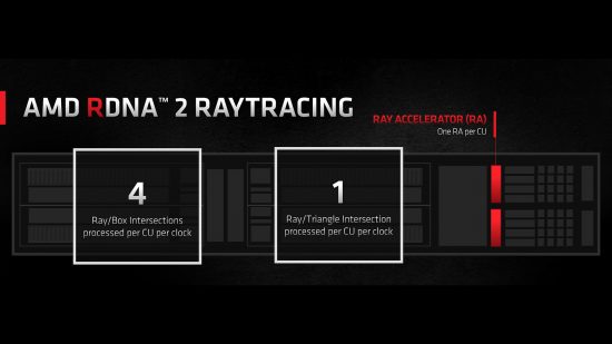
Each CU in RDNA 2 contains one RA (two per dual CU configuration), so the number of RAs will scale in line with the reduction in CUs you’ll see in the RX 6800 XT and RX 6800. This is much like Nvidia’s configuration, with RT cores scaling with its Streaming Multiprocessor clusters. Also, like Nvidia’s approach, the Ray Accelerators only perform ray-box and ray-triangle intersection testing and not Bounding Volume Hierarchy (BVH) traversal, with that task taken on by the CUs.
As a quick refresher, ray tracing works by calculating if a ray of light intersects with a triangle. However, to improve performance, before triangle intersection is tested, first a bounding volume check is performed – a bounding box is a simple cuboid that encompasses a complex model that can be made up of many triangles. It’s these two core tasks that are accelerated by the RA cores.
Another crucial step in ray-tracing calculations is traversing bounding volume hierarchies (a tree-like structure defining which bounding volumes fit within which other larger bounding volumes – a Russian doll of bounding volumes, as it were). However, neither AMD nor Nvidia’s ray-tracing cores yet perform this function, with this instead performed on the usual stream processors.
AMD has specified that each RA unit can process four ray/box intersections per clock and one ray/triangle intersection per clock, which doesn’t mean a great deal when compared with Nvidia’s RT cores, as Nvidia hasn’t specified these numbers. Nvidia has only said that the new RT cores in Ampere can perform twice as many of these operations as its 1st-generation cores. Sure enough, despite Navi 21 having 80 RA cores compared to Ampere’s 84 RT cores, Nvidia still has a significant advantage in ray-tracing speed, as evidenced by our testing (see p16).
Ray tracing is actually another area where RDNA 2’s Infinity Cache comes into play, as this large data pool can hold a ‘very high percentage’ of the BVH working set, which minimises the potential latency of intersection calculations on that set. Plus, of course, having any sort of dedicated hardware provides a big leap over software-based ray tracing, with AMD citing a 10x performance improvement for the tasks its RA cores do accelerate.
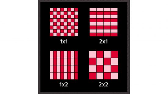
While it’s certainly the most prominent one, ray tracing isn’t the only feature to arrive with DirectX 12 Ultimate. Another crucial tool for developers will be variable rate shading (VRS). This is where instead of a pixel shader shading just one pixel it can be assigned to cover up to 16 (4×4) pixels. In practice, 16 pixels is an extreme example, and more common will be to have a single pixel shader value shared across two (2×1 or 1×2) or four (2×2) pixels.
It’s this smaller subset of coarse pixel configurations that RDNA 2 supports. The advantage here isn’t so much that this software feature is accelerated in hardware, but simply that the hardware supports the feature at all, allowing developers to implement VRS in games, where it provides an inherent performance advantage.
It’s a similar situation with Mesh Shading, another new addition with DirectX 12 Ultimate. This is a significant feature that sees a complete reworking of the front end of the graphics pipeline. Whereas previously the meshes of triangles that describe the surface of a 3D object had to be processed in one lump for any given mesh, with mesh shading the whole mesh can be broken down and processed in parallel.
This ability to break down and apply extra processing to a mesh also makes it easy to incorporate geometry modifications such as tessellation. Again, though, we’re not talking about a specific task that’s sped up by the GPU in such a way that would allow for an apples-to-apples performance comparison, but simply that the new GPU is able to provide these new software features.
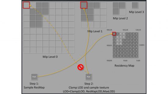
The penultimate piece of this new feature puzzle is Sampler Feedback. This is a framework that allows the graphics pipeline to keep track of the method and details of a texture sampling call. This is useful for when a scene might rapidly require a texture to be sampled at different rates (using texture mipmap streaming). By keeping track of what’s being sampled, the system is able to keep more granular control over what sections of a mipmapped texture (textures in modern games can be very large!) are loaded into memory, reducing the memory footprint.
DirectStorage is the final major notable DirectX 12 Ultimate feature that’s newly supported with RDNA 2. This in essence allows a GPU to directly access the latest ultra-fast NVMe SSDs, bypassing the overheads that were inherent with previous storage APIs. The most obvious benefit of this will be reduced game load times, as data is able to stream straight into the GPU much more rapidly. However, there will also be potential improvements in performance in situations such as where massive amounts of texture data is being streamed into and out of a graphics card’s memory.
RDNA 2 Smart Access memory and FidelityFX software
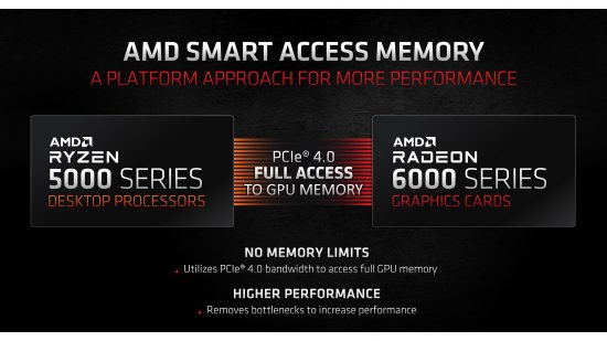
Outside of DirectX 12 Ultimate features, there’s a handful of other miscellaneous improvements and features in or coming to RDNA 2. The first is Smart Access memory, which circumvents the current 256MB limit that CPUs have for accessing GPU memory. Currently, only available with AMD Ryzen 5000-series CPUs and RDNA 2 GPUs, this BIOS-enabled feature will allow a CPU to tap directly into a graphic card’s full bank of GDDR6 memory, providing a small (up to 11 percent) performance uplift.
AMD has also announced its FidelityFX suite of software features, which will be available to developers. Consisting of seven image quality enhancing tools – including VRS support – it’s basically an all-in-one, branded suite of tools to highlight to developers the extra effects that can be implemented with RDNA and RDNA 2. One key forthcoming feature is called Super Resolution, which looks as though it may work similarly to Nvidia’s DLSS technology.
The future for AMD graphics cards
We’ve seen from our performance testing that RDNA 2 does deliver on everything AMD has promised. The massive gains in performance, power efficiency and features have put the company’s graphics cards right back into contention, but there are clearly still some areas that need improvement.
Ray-tracing performance is notably behind Nvidia, so we’d hope to see a straight beefing up of its RA cores in subsequent iterations of RDNA. How easy that might be and how Nvidia will respond is anyone’s guess, but given the adequate performance RTX 30-series cards provide already, simply reaching parity with Nvidia’s current cards would be a significant step up for AMD.
It will also be interesting to see how Infinity Cache scales both for smaller configurations of RDNA 2 and for future ‘RDNA 3’ designs. Is a massive cache the way forward from now on, or just a workaround for this generation? We certainly look forward to finding out.
