
The latest AMD Radeon GPU architecture is called RDNA 3, and it has the potential to provide some serious competition for the Nvidia Ada architecture if AMD can get the pricing right. After several years of struggling in terms of both performance and power efficiency with its GPU designs, the arrival of AMD’s 1st-generation RDNA architecture saw the company leap forward in both areas.
The RDNA 2 architecture continued this trend, with a hefty 54 percent improvement in performance per watt and the introduction of support for ray tracing. It made AMD’s Radeon RX 6000-series graphics cards, such as the AMD Radeon RX 6750 XT, compelling mid-range alternatives to the Nvidia GeForce RTX 3000 series, especially for non-AAA titles that didn’t take advantage of ray tracing.
Now AMD’s back with RDNA 3, which rather pleasingly brings with it the exact same claimed 54 percent increase in performance per watt, with AMD promising that RDNA 3 will improve ray tracing performance by 50 percent compared to RDNA 2.
We’ve seen the result of these improvements in our reviews of the AMD Radeon RX 7900 XTX, as well as the AMD Radeon RX 7900 XT, which take big leaps in both non-ray traced and ray-traced performance over the previous-generation Radeon RX 6000-series GPUs. You can now also read our full AMD Radeon RX 7600 review.
Also new to this iteration of the architecture is the addition of an AI accelerator, which provides dedicated hardware for speeding up the matrix multiply assist operations generally associated with machine learning tasks. These accelerators are the equivalent of Nvidia’s Tensor cores, and their introduction means AMD finally has feature parity (if not outright performance parity) for the big duo of features Nvidia first introduced with its GeForce RTX 2000-series GPUs.

For gamers, these AI accelerators won’t currently bring much to the table, as AMD doesn’t have an AI-accelerated equivalent of Nvidia’s DLSS technology, and currently this is the only gaming feature that uses Tensor cores.
Other notable changes include RDNA 3 using TSMC’s 5nm and 6nm production processes, rather than the 7nm process of AMD’s RDNA 2 chips. This compares with Nvidia’s use of TSMC’s very latest ‘4nm’ process for its GeForce RTX 4000-series GPUs, such as the Nvidia GeForce RTX 4090.
That 4nm process is a refinement of the company’s 5nm process, boasting up to an 11 percent uptick in performance, 6 percent higher transistor density, and a 22 percent boost in power efficiency over its 5nm process.

The first GPU to implement the RDNA 3 architecture is the Navi 31, which houses 58 billion transistors and boasts 61 TFLOPS of performance, according to AMD. These mark significant increases over the 26.3 billion transistors and claimed 12.8 TFLOPS of performance for the previous-generation Navi 21 chip, which was used in the AMD Radeon RX 6950 XT.
However, the new Nvidia AD102 GPU that sits at the heart of the GeForce RTX 4090 packs a massive total of 76 billion transistors, with Nvidia claiming 83 TFLOPS of processing power; figures that make its relatively reasonable power consumption all the more impressive. Meanwhile, the AD103 GPU of the GeForce RTX 4080 houses just 46 billion transistors.

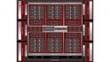
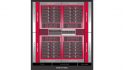
The Radeon RX 7900 XTX and XT
To quickly recap, Navi 31 is initially available in the two graphics card configurations we’ve reviewed this month – the Radeon RX 7900 XTX and 7900 XT. The former is the flagship card and it packs 96 of the architecture’s compute units (CUs), providing 6,144 dual-issue stream processors (SPs), 192 AI accelerators, and 96 ray tracing RT cores. It’s coupled with 24GB of GDDR6 VRAM accessed via a 384-bit memory interface, and AMD’s quoted game clock speed is 2.3GHz.
Meanwhile, the Radeon RX 7900 XT has 12 fewer CUs than the 7900 XTX, resulting in a total of 5,376 dual-issue stream processors (we’ll cover what we mean by ‘dual’ later), 168 AI accelerators and 84 2nd-generation RT cores. It also uses one fewer memory cache die, resulting in a narrower 320-bit interface that communicates with the card’s 20GB of GDDR6 VRAM. AMD’s quoted game clock speed for this GPU is 2GHz.
In comparison, the previous-generation Radeon RX 6950 XT has just 80 CUs providing 5,120 stream processors, no AI accelerators and 80 1st-generation RT cores. That GPU was coupled with 16GB of GDDR6 VRAM, accessed through a 256-bit memory interface, and the game clock was 2.1GHz.

As for comparisons with Nvidia’s latest cards, differences in architecture mean it’s not entirely meaningful to compare the numbers of its CUDA cores (equivalent of stream processors), Tensor cores (equivalent of AI accelerators), and RT cores but it helps to differentiate between Nvidia GPUs. As such, the RTX 4090 packs in 16,384 CUDA cores, 512 Tensor cores, and 128 RT cores. The card runs at a 2235MHz base clock with a boost clock speed of 2565MHz.
Meanwhile, the RTX 4080 has considerably less power on paper, with 9,728 CUDA cores, 304 Tensor cores and 76 RT cores. Like the RTX 4090, though, it boasts high peak clock speeds, with a boost clock of 2505MHz and base clock of 2205MHz.
It’s also the case that the new Radeon RX 7900-series reference cards are much more compact than the equivalent GeForce RTX 4000-series cards, and the AMD cards don’t require the new infamously melty 16-pin power connector of the Nvidia cards either, instead relying on two 8-pin PCIe connectors.

We’re now going to dive head first into the inner workings of RDNA 3, but before we do so we’d like to introduce you to the slide carousel below, which enables you to view the diagrams and slides we’ve used throughout the feature, and you can click on the ones in the carousel to view them in more detail.


Chiplet challenge
The most prominent feature of the new RDNA 3 architecture is its use of not just new manufacturing processes when compared with RDNA 2, but the use of a chiplet design. Instead of having a single die that encompasses all the main functions of the GPU, as on all previous graphics cards of the past 20 or so years, RDNA 3 uses a single large Graphics Compute Die (GCD) and up to six smaller Memory Cache Dies (MCDs).
The GCD takes care of most of the functions you’d normally associate with a GPU, with all the CUs, RT cores, video encoders and more being housed in that chip. All that has been separated out from the main GPU is the Infinity Cache (a large L3 cache) and the memory interface.
This arrangement runs contrary to a popular rumor in the run-up to the RDNA 3 launch, which speculated that the upcoming chiplet GPU design would split up the processing portions of the GPU and essentially function in the same way as two graphics cards when using AMD CrossFire or Nvidia SLI. That may be a future feature of chiplet GPU design, but for now, it’s just the caches and memory interface that have been separated from the main GPU die.

While only removing the cache and memory interface may not seem like the most significant silicon-saving measure, modern GPUs have large last-level caches and highly sophisticated memory controllers that take up a large portion of a chip. The Infinity Cache of Navi 31 and the L2 cache of the RTX 4090 are both 96MB, which is hefty for an on-die cache. As such, removing these components reduces the size of the rest of the GPU by a significant amount.
Specifically, by moving these functions to its MCDs, the GCD of Navi 31 has been kept to just 300mm², which compares to 520mm² for the previous-generation Navi 21 GPU. Meanwhile, the AD102 silicon of the GeForce RTX 4090 has a whopping die area of 609mm², although the AD103 GPU of the GeForce RTX 4080 has a much more modest 379mm² die area.
Each of Navi 31’s MCDs measures a tiny 37mm² for a combined total of area of 222mm² when using a full count of six MCDs. Add that to the 300mm² are of the CGD and that’s a total die area that’s slightly larger than the single die of Navi 21, and much larger than Nvidia’s AD103 die, though still markedly smaller than AD102.
Having a combined total die area that’s no smaller than a previous GPU design may not seem like it’s gaining you much overall. However, not only are both the transistors in the GCDs and MCDs of Navi 31 much more densely packed than in Navi 21 – thanks to smaller manufacturing processes, but there are also several other big advantages to producing a total die area via several smaller dies rather than via one big die.

The first advantage is that even a small reduction in the size of a silicon chip results in the ability to produce significantly more dies per silicon wafer, reducing relative cost and improving yields.
For instance, if we perform some rough calculations using a silicon wafer yield calculator, while a typical 300mm-diameter silicon wafer could produce in the region of 89 AD102 GPUs – assuming no defects and a perfect yield – that same wafer could produce 190 Navi 31 GCDs or 1,645 MCDs. That’s a heck of a lot more complete Navi 31 chips per wafer than AD102 when averaged out over hundreds of wafers.
Once you factor defects into the equation the situation becomes even more dramatic. While not all defects will render a die unusable – depending on where the defect lands, that portion of the chip can sometimes be disabled and the rest of the chip used for a lower-tier GPU – getting complete, defect-free dies is the most desirable outcome.
As such, when we include the nominal defect rate of 0.09 defects/cm² for TSMC’s 6nm process (just as an example – these chips are all produced on slightly different processes, after all), you arrive at a yield of just 46 perfect AD102 GPUs, 138 GCDs and 1556 MCDs per 300mm wafer. Or, to look at it another way, the yield percentage rate – the ratio of good to bad dies – of those same three chips is 58.5 percent, 76.8 percent and 96.7 percent. It’s massively more efficient to produce smaller dies.

The other big upside to a chiplet design approach is the ability to use different manufacturing processes for different portions of the chip, which is precisely what AMD has done. While the GCDs are produced on TSMC’s smaller, more up-to-date and more expensive 5nm process, the MCDs are produced on the slightly larger, older and cheaper 6nm process.
Not only does this allow for potential cost savings for producing the MCDs, but it reduces the dependency of AMD on being allocated production time on the latest and most sought-after manufacturing processes. In contrast, not only will Nvidia have had to spend big money to even secure first access to TSMC’s very latest ‘4nm’ process, but it will be in some ways wasting that cutting-edge process allocation by producing the entirety of its GPUs on that process.
There are some downsides to the chiplet approach though. For a start, while using different manufacturing processes brings potential costs and manufacturing efficiency benefits, it does mean the MCDs don’t benefit from the power-saving and higher-performance capabilities of the newer 5nm process, let alone the 4nm process Nvidia is using. However, according to AMD, the components on the MCDs don’t scale all that well compared with the GCD components, so there’s very little benefit to shrinking them anyway.
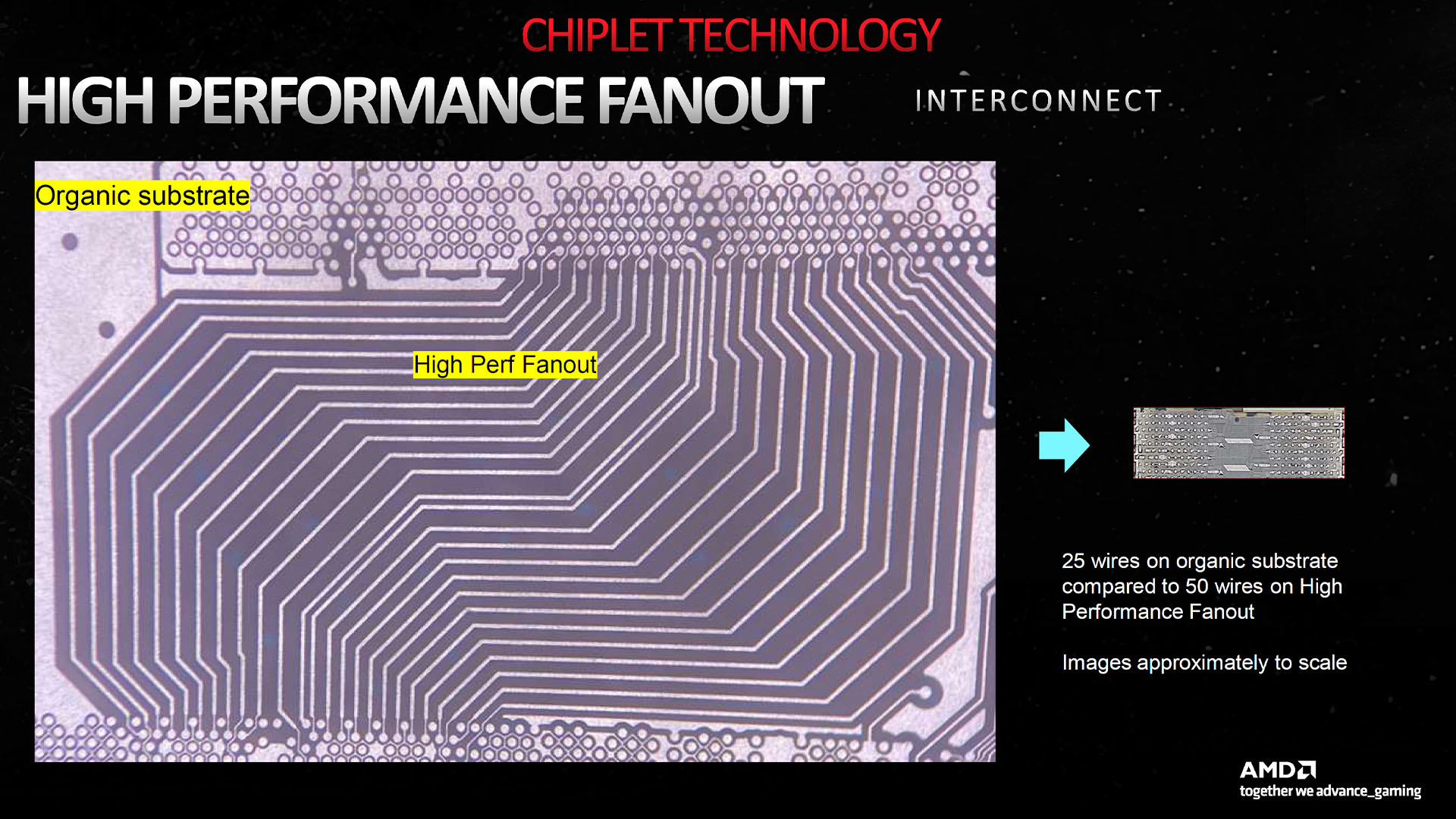
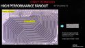
The other big hurdle to overcome is assembling the seven different dies into one chip package and getting them to communicate correctly and speedily. Inter-die communication presents an inherent difficulty, and it’s one that’s significantly greater when dealing with the thousands of internal connections of a GPU as compared to the hundreds of connections required within a chiplet-based CPU design. To overcome this, AMD has introduced a new interconnect system called Infinity Fanout Links.

Infinity Fanout Links is essentially a high-density PCB trace on an interposer layer that’s far smaller than previous chiplet interconnect designs. In one of its slides AMD shows the example of the PCB connections used on one of its CPUs compared with the new Infinity Links, and the difference in density is enormous – 10x.
The image is also slightly mislabelled (by AMD) – the yellow labels are too far over to the left and should instead be showing that the larger image is the older PCB trace on an organic substrate, while the high-performance Infinity Fanout Links system is to the bottom right.
As well as allowing for a massive increase in connection density, Infinity Fanout Links had to be power-efficient – external links are almost always more power-hungry than on-die connections – and sure enough AMD claims a saving of up to 80 percent in power consumption when using Infinity Fanout Links over the previous organic package link used for its CPUs. AMD claims the interconnect consumes less than 5 percent of the GPU’s total power.
As for the resultant bandwidth of this new interconnect, it stands at a ridiculous figure of 5.3TB/sec. This bandwidth is shared out among the six MCDs, so it will scale accordingly if any MCDs are disabled.
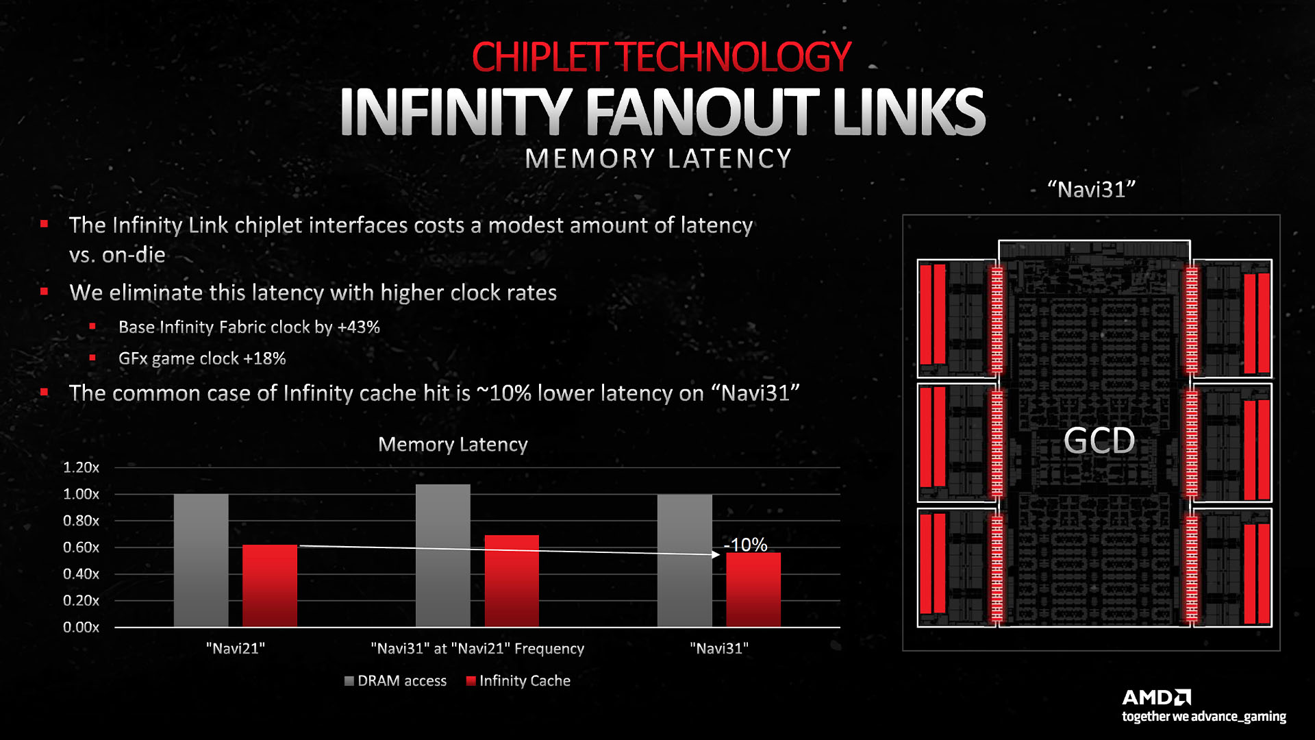
One downside of Infinity Fanout Links is an increase in latency over using an on-die cache.
To get around this latency, AMD has simply cranked up the clock speed of the Infinity Fabric by 43 percent to achieve the same overall cache latency as on Navi 21. The company has also optimized the cache for better data reuse, ensuring higher cache hit rates, which results in quicker delivery of data to the GCD, while using less power than having to make a request to the graphics card’s RAM.
Communications to that memory are made via a dedicated 64-bit path from each MCD, for a combined total of 384 bits for the memory interface, which is coincidentally exactly the same width as the memory interface on Nvidia’s GeForce RTX 4090. One or more of the MCDs can be disabled to produce a lower-tier graphics card, with the memory bus width lowering accordingly – the Radeon RX 7900 XT has one MCD disabled and has a 320-bit memory interface.

Inside the AMD RDNA 3 core
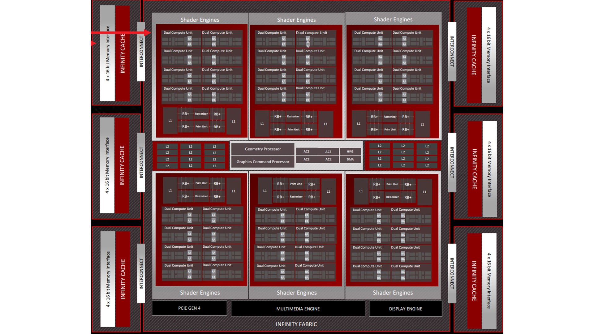
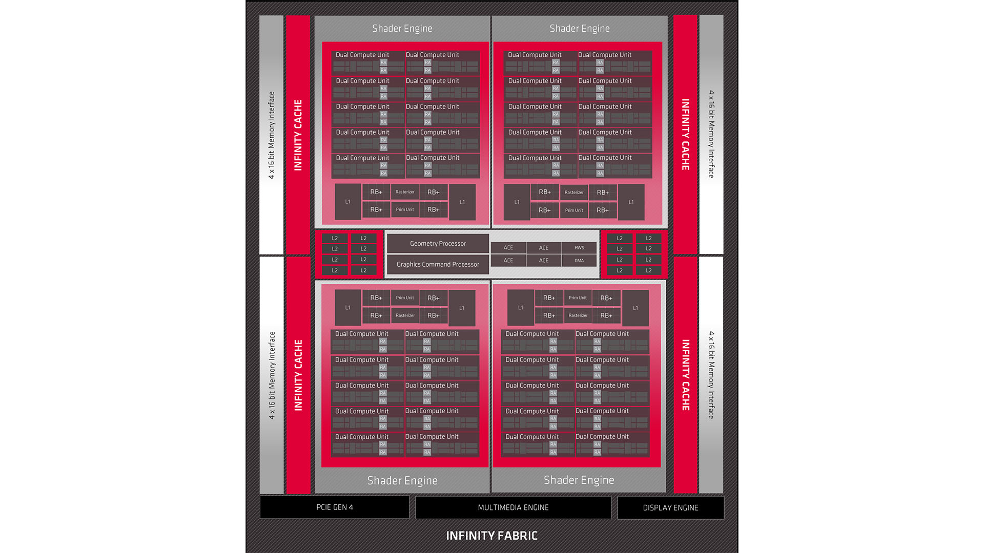
The GCD of Navi 31 is architecturally similar to the previous RDNA 2 GPU design. If we compare the block diagrams of Navi 31 (above) with Navi 21 (below), we can see that the overarching layout is much the same.
Large clusters of compute units are stacked either side of a central graphics command processor, a geometry processor, various other specialist function blocks and blocks of L2 cache. The graphics command processor controls issuing of instructions to the rest of the GPU.

The compute units are packaged up into six sections of 16 compute units (technically packaged as eight dual-compute units), each of which is called a shader engine by AMD. The GPU will distribute workloads in bulk to each of these shader engines, which they will process in parallel.
Also packed into each Shader Engine are portions of L1 cache, the render backends and rasterizers.
This structure is similar to RDNA 2, except the older design packaged 20 compute units into four shader engines for a total of 80 compute units, whereas Navi 31 has 16 compute units per shader engine and six engines, totaling 96 compute units.
That relatively small 20 percent increase in the total number of CUs is a bit of a surprise given the large uptick in performance we see between the Radeon RX 6950 XT and the Radeon RX 7900 XTX, especially when we compare this to the increase in the number of CUDA cores from Nvidia’s GeForce RTX 3090 Ti to the RTX 4090. The former packed in 10,752 while the latter bumped this to 16,384, for a 52 percent increase.
The answer to why so much more performance has been gleaned from such a similar number of CUs is, not surprisingly, that the CUs are much more capable than the ones in the older RDNA 2 architecture. What’s more, many other enhancements have been made to the rest of the architecture and the whole chip in order to keep those CUs running faster and more efficiently.
Chief among these enhancements is a boost in clock speeds, with AMD claiming that RDNA 3 can in theory boost all the way up to 3GHz. That’s far faster than the boost clock speeds used on the company’s reference cards, but third-party cards and future, refined GPUs could open up the taps. Power consumption and heat will rise but, depending on the performance uplift, this might be deemed worthwhile for those seeking raw power above all else.
AMD has also decoupled the clock speeds of the front end of the graphics pipeline from the shader engine. While the Radeon RX 7900 XTX is rated to run at a game clock of 2.3GHz, its front-end clock speed is actually 2.5GHz. AMD claims pulling back the shader engine speed by just 9 percent saves 25 percent on power consumption. As for the Radeon RX 7900 XT, it has a quoted game clock speed of 2GHz but front end clock speed of 2.4GHz.
When it comes to power consumption, AMD claims RDNA 3 can run at half the power of RDNA 2 while providing the same performance, or it can hit 1.3x the frequency while using the same power.
Other overarching improvements include an increase in silicon utilization of approximately 20 percent. Silicon that’s left unused for whatever reason – perhaps because the feature is deprecated or the architecture is inefficient for typical modern workloads – is wasted space and power, so by trimming the fat AMD can free up space for more useful silicon features, or at the very least just reduce the size of the die further.

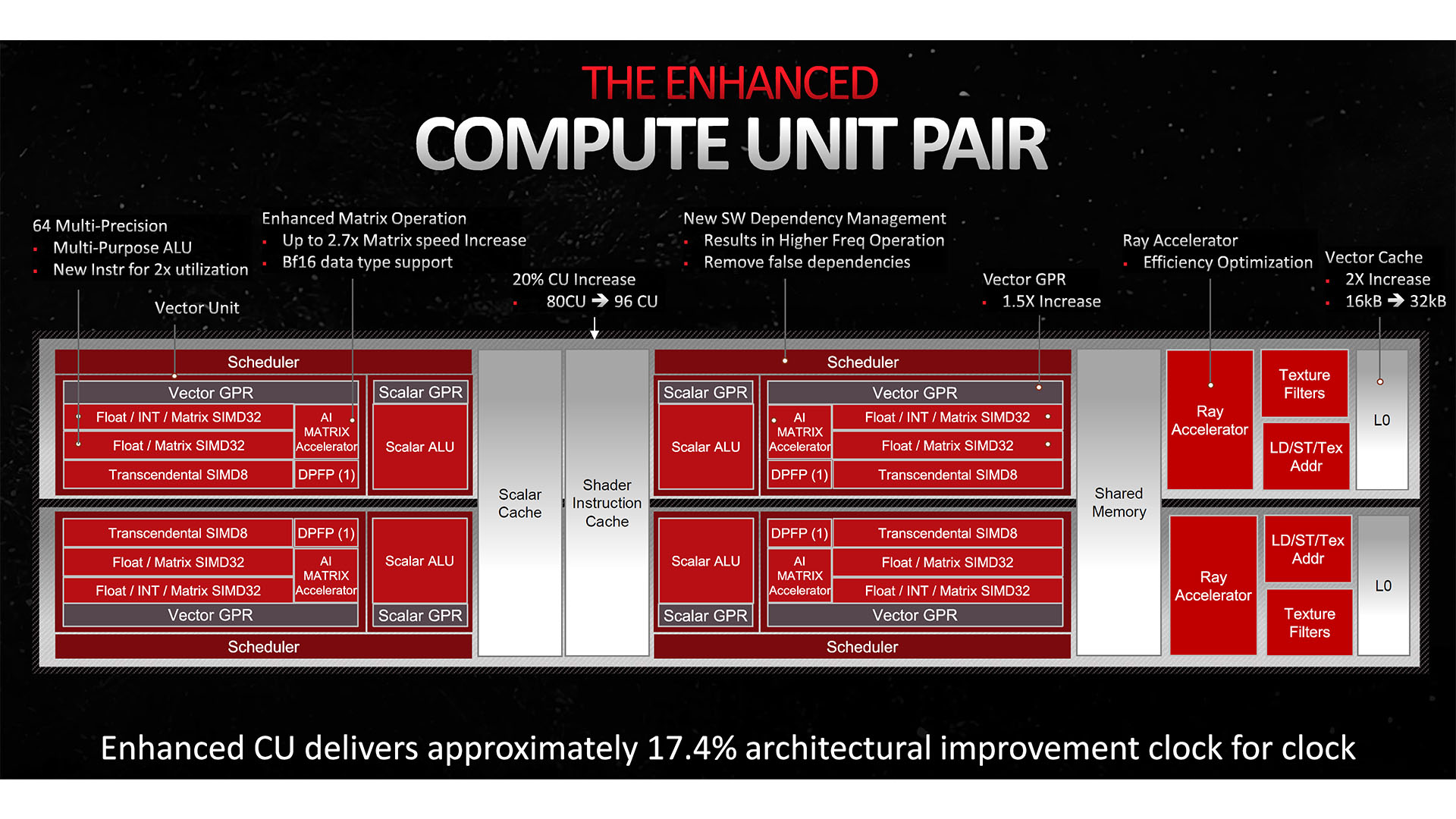
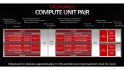
A new compute unit
The compute unit, or CU, is the beating heart of the RDNA 3 architecture, with each CU housing a stack of stream processors for crunching through the massive amounts of parallel processes that are the grunt work of any GPU.
Also included in each CU are two of AMD’s new AI accelerators, a 2nd-gen RT accelerator, texture filling and address units and a vector cache. Always arranged in pairs, each CU shares a scalar cache, shader instruction cache and memory block with its neighbor to form a CU pair, or dual CU.
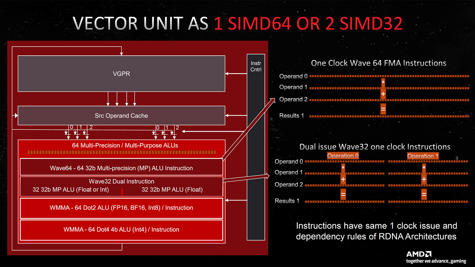
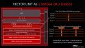
On the surface, not all that much appears to have changed when comparing the CUs of RDNA 2 to RDNA 3. However, there are in fact big changes throughout the design. The single biggest change is the addition to each vector unit (a block of stream processors that work on a single task in parallel) of a second SIMD32 block, which contains 64 stream processors dedicated to floating point and matrix workloads.
This essentially doubles the stream processor count of each CU, from 64 to 128, and in turn the floating point performance of each CU. However, because this new block doesn’t perform integer operations, it isn’t strictly a full duplication of the existing stream processor setup.
This has led to a confusing situation whereby AMD has sometimes referred to each CU as still having 64 stream processors and resultingly Navi 31 having 6,144 stream processors, and sometimes referring to it as having 128 stream processors per CU for a total of 12,288.

Both figures are technically correct, depending on your parameters, but it’s the former figure that tallies more with the 17.4 percent clock-for-clock performance uptick of the new CU compared with RDNA 2. If it was a full doubling of the stream processor count, we’d expect to see closer to double the clock-for-clock performance.
That said, the higher figure bears a greater resemblance to how Nvidia’s Ada Lovelace architecture is laid out, with it housing 128 FP32 CUDA cores per Streaming Multiprocessor (SM), along with 64 dedicated INT32 units.
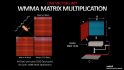
Other enhancements to RDNA 3’s CUs include the addition of those dedicated AI Matrix Accelerators, which include support for BF16 (brain-float 16-bit) and INT4 WMMA Dot4 (Wave Matrix Multiply Accumulate) instructions.

This unit works in conjunction with the vector units to perform matrix operations, rather than taking over the task completely, but the net result is a 2.7x increase in matrix workload performance per CU, which should help the uptake of AMD GPUs for professional use.
Also included is a 50 percent increase in the size of the general-purpose vector register for each vector unit, along with a larger shared L0 vector cache. This ensures that each CU simply has more space for data and instructions to be kept as close to the stream processors as possible, saving the GPU requesting data from slower stores elsewhere on the chip.

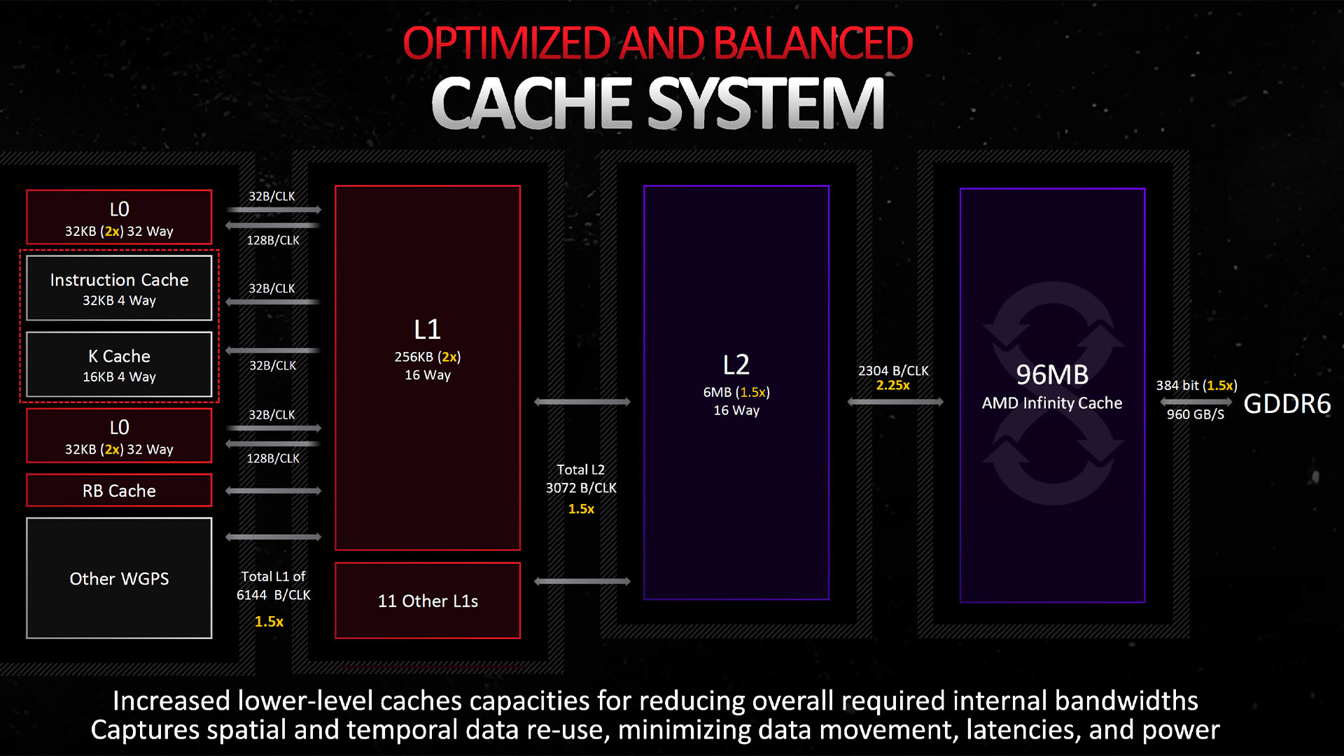
RDNA 3 cache changes
As we just mentioned, the L0 cache of each CU vector unit has seen a doubling in size from 16KB to 32KB, but this is only part of an overhaul of RDNA 3’s cache structure compared to its predecessor. The L1 caches – housed alongside and dedicated to each block of eight dual compute units inside each shader engine – have also doubled in size from 128KB to 256KB. while the L2 cache that’s shared across the whole GPU is 50 percent larger, up from 4MB to 6MB.
An interesting twist on this theme of increasing cache sizes is that the L3 or Infinity Cache has actually dropped in size from 128MB to 96MB, compared to RDNA 2. This is particularly intriguing given the offloading of Infinity Cache onto the MCD chiplets. Intuitively, you might expect that having space on a separate die would open up the opportunity to have an even larger cache, but clearly, AMD feels it’s not needed.

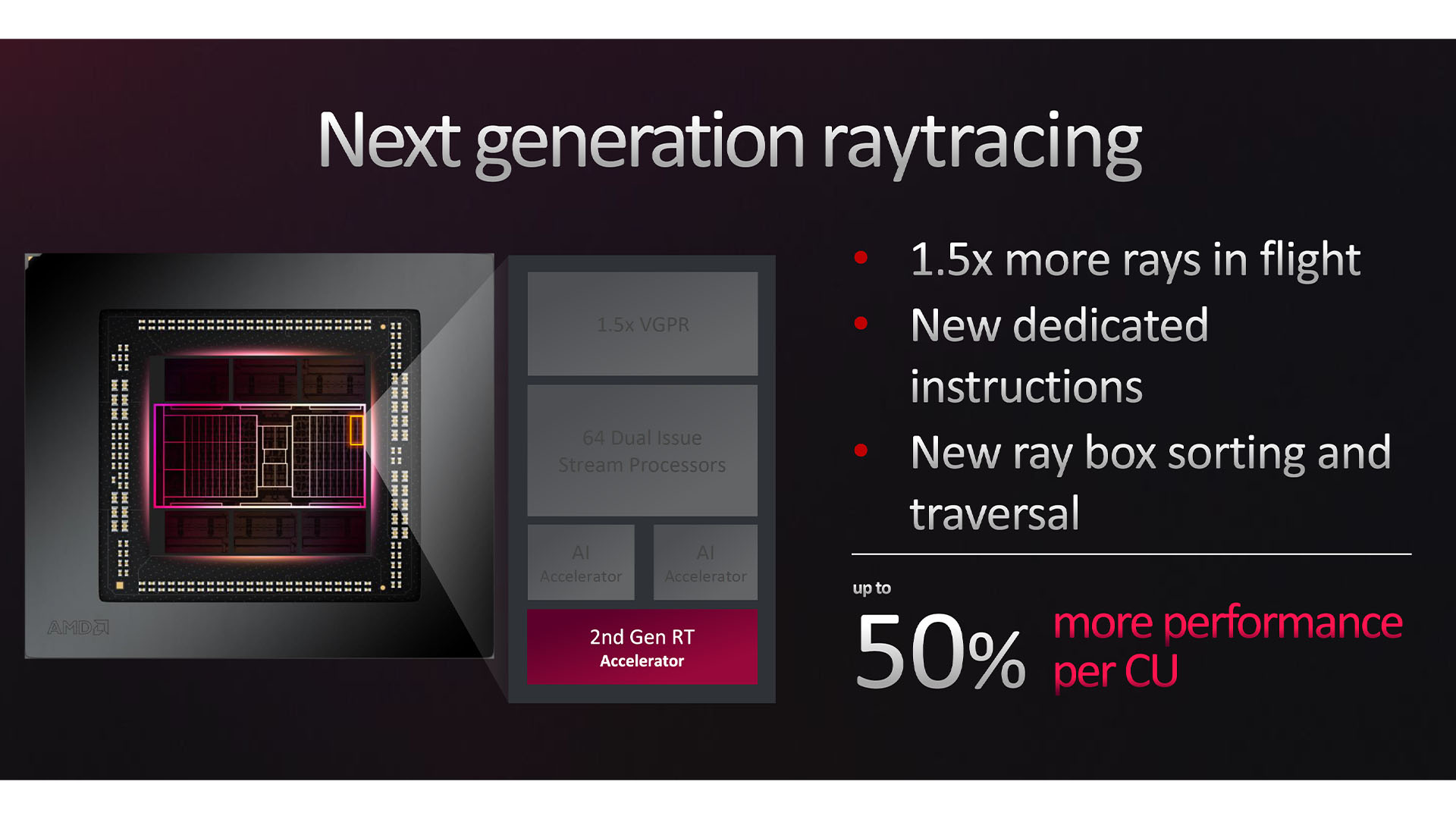
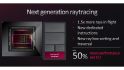
AMD RDNA 3 2nd-gen ray tracing core
For many users, the most appealing part of RDNA 3 will be its significantly bolstered ray tracing performance, which AMD claims has improved by up to 80 percent for some tasks when compared to RDNA 2.
In our tests, while Nvidia still maintains a strong lead on this front thanks to its RTX 4000-series GPUs based on the new Ada architecture, the Radeon RX 7900 XTX does trade blows with Nvidia’s Ampere-based GeForce RTX 3000-series cards, including the top-end RTX 3090 Ti.
Powering that improvement is an RT accelerator that offloads some of the overall ray tracing workload, while also incorporating several improvements to existing accelerated tasks.
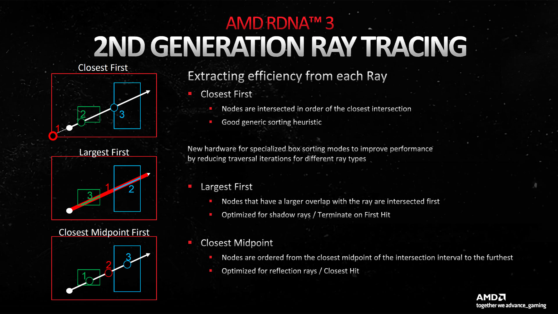
Specifically, the new ray tracing accelerator now incorporates a degree of hardware bounding volume hierarchy (BVH) sorting and traversal, a feature that was previously fully performed on the GPU’s general shader hardware in RDNA 2 designs. This move can reduce shader instruction count requirements by up to a factor of 15x.

Other enhancements include more efficient ray calculation culling, eliminating any unnecessary work as early as possible. New algorithm options for calculating ray/volume intersections also allow for optimization of the workflow, depending on the type of ray tracing function being performed. If you’re calculating ray-traced shadows, for instance, you can prioritize volumes that are largest first, while reflection ray functions can prioritize the closest midpoint, or the default of using the closest intersection can be used.
Also of significant help to overall ray tracing performance are all those increased cache sizes we mentioned earlier. The larger VGPR in particular enables 50 percent more rays to be in flight at once, greatly reducing the need to drop to slower, higher-level caches in order to find the required data.
AMD RDNA 3 deep dive
Along with its several large, obvious changes over its predecessor, RDNA 3 also incorporates a host of tweaks to the underlying architecture of the rest of the GPU. The first of these is improved handling of primitives via a new Multi-Draw-Indirect accelerator.
Primitives are the fundamental shapes used to construct the surfaces in a 3D scene – most often triangles – and initial handling of them is undertaken by the CPU. As such, the new accelerator looks to take a load off the processor, reducing CPU and driver overhead in the process.
Primitive culling – the act of reducing the number of triangles to pass on for further calculations by establishing whether they’re no longer needed (because they’re obscured by another object in the scene, for instance) – is also accelerated, helping to again reduce potential CPU/software culling overhead.
Other changes include a claimed 50 percent increase in rasterization performance, with up to six peak primitive and 192 peak pixels of rasterization per clock cycle – this should be particularly beneficial for running games at very high resolutions. RDNA 3 also adds out-of-order exports from the pixel shader, which allows for tasks to be more efficiently kept running through the GPU, and not held up while one task is waiting to be completed.

AMD RDNA 3 display and media engines
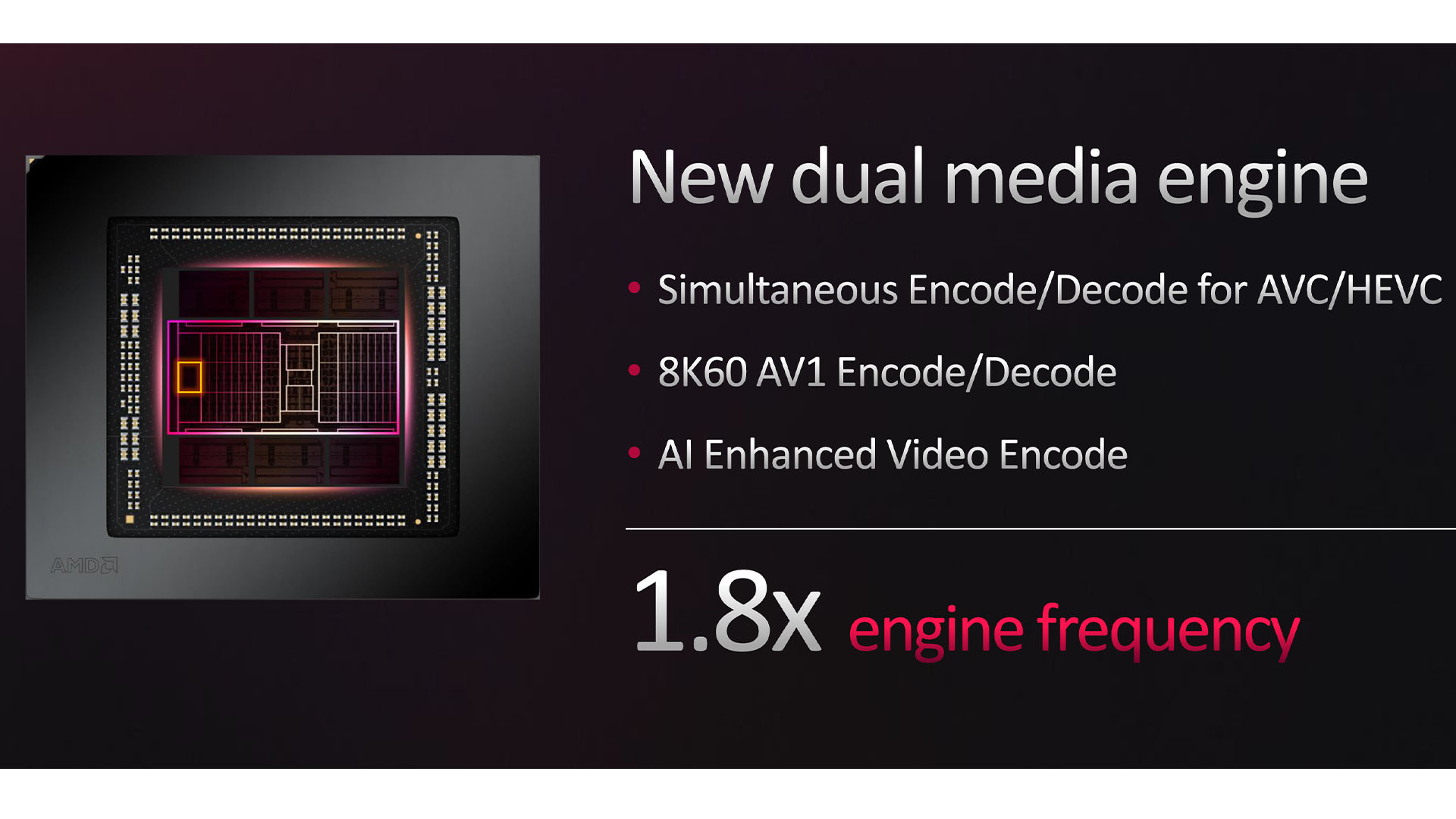
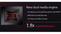
One of the areas where AMD has been trailing Nvidia lately is video encoding and decoding, and that’s an area the company is hoping to improve with the new media engine of RDNA 3. It supports the latest AV1 compression encoder and boasts improved H.264 (AVC) and H.265 HEVC encode/decode performance, with simultaneous encode/decode of the latter.
These improvements come in part from taking advantage of the new AI accelerators, while the whole media engine runs at 1.8x the frequency of RDNA 2. Another key area of improvement is support for DisplayPort 2.1 with ultra-high bandwidth support, which enables the GPU to output a display at ridiculous resolution/refresh rate combinations, such as 8K at 165Hz or 4K resolution at 480Hz.
Such futureproof connections might look good on paper, but good luck trying to get any games to run at those settings. Along with two of these DisplayPort 2.1 ports, the reference card designs also include an HDMI port and a USB-C output, providing a wide range of output configurations.
Final thoughts
We’ve been impressed by AMD’s RDNA 3 architecture for the most part. There are some disappointments – there’s currently nothing that uses the new WMMA units, the ray tracing performance isn’t as good as Nvidia’s latest Ada GPUs, and there’s no AI frame generation tech, such as DLSS 3.
However, the price of the Radeon RX 7900 XTX has now dipped below the $1,000 mark, and this GPU’s ray tracing performance is still right up there with Nvidia’s last-gen flagship, the GeForce RTX 3090 Ti. If ray tracing is a ‘nice-to-have’ feature, rather than a ‘must have’ one, then this is an awesome GPU for 4K gaming – the rasterization performance is amazing for the money.
We hope you’ve enjoyed taking a deep dive into the AMD RDNA 3 GPU architecture with us. If you’re on the lookout for a new graphics card, then check out our full guide to the best graphics card, where we list several options at a range of prices.