The latest AMD CPU architecture is called Zen 4, and it sees AMD mounting a full-frontal assault on Intel with its Ryzen 7000 series of CPUs. While AMD has garnered a significant amount of good will from the PC-buying public, thanks to its previous Ryzen processors pushing forward progress on CPU performance, pricing and platform longevity, when it comes to putting your money where your mouth is, most buyers will go where they can get the best bang for their buck.
It’s good for AMD, then, that the new chips, such as the AMD Ryzen 7 7700X, well and truly deliver on their performance promise – two of the chips are featured on our full guide to the best gaming CPU. But what makes them tick and what other features are hidden away inside AMD’s latest CPUs? Let’s take a closer look.
The AMD Zen 4 platform and lineup
Before we delve too deep into the architecture of Zen 4 itself, let’s quickly recap which processors we’re discussing here, which features the chips include and the other key products alongside them.
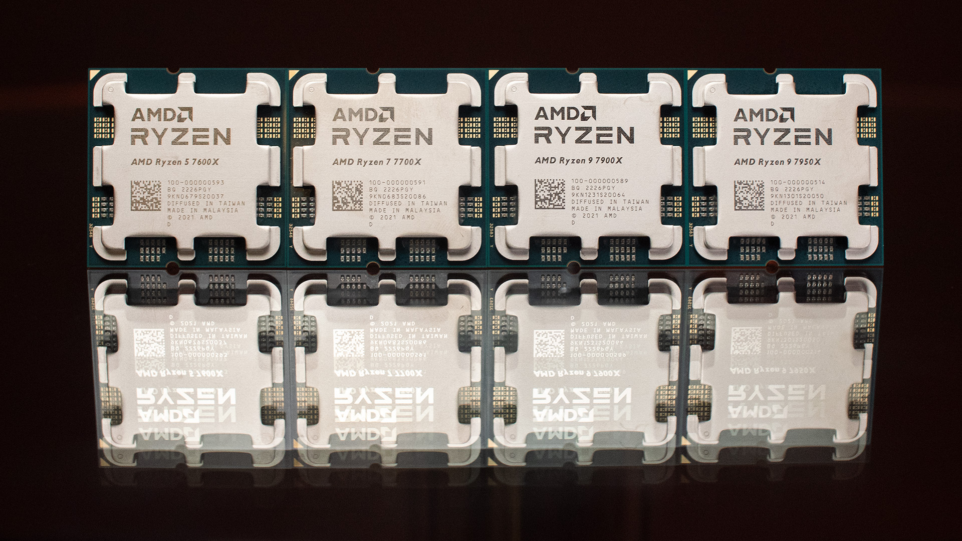
There were four Ryzen 7000-series CPUs in the initial launch roster – the 16-core Ryzen 9 7950X, the 12-core Ryzen 9 7900X, the 8-core Ryzen 7 7770X and the 6-core Ryzen 5 7600X. All these CPUs support Simultaneous Multithreading (SMT), so can have twice as many application threads in flight as they have cores.
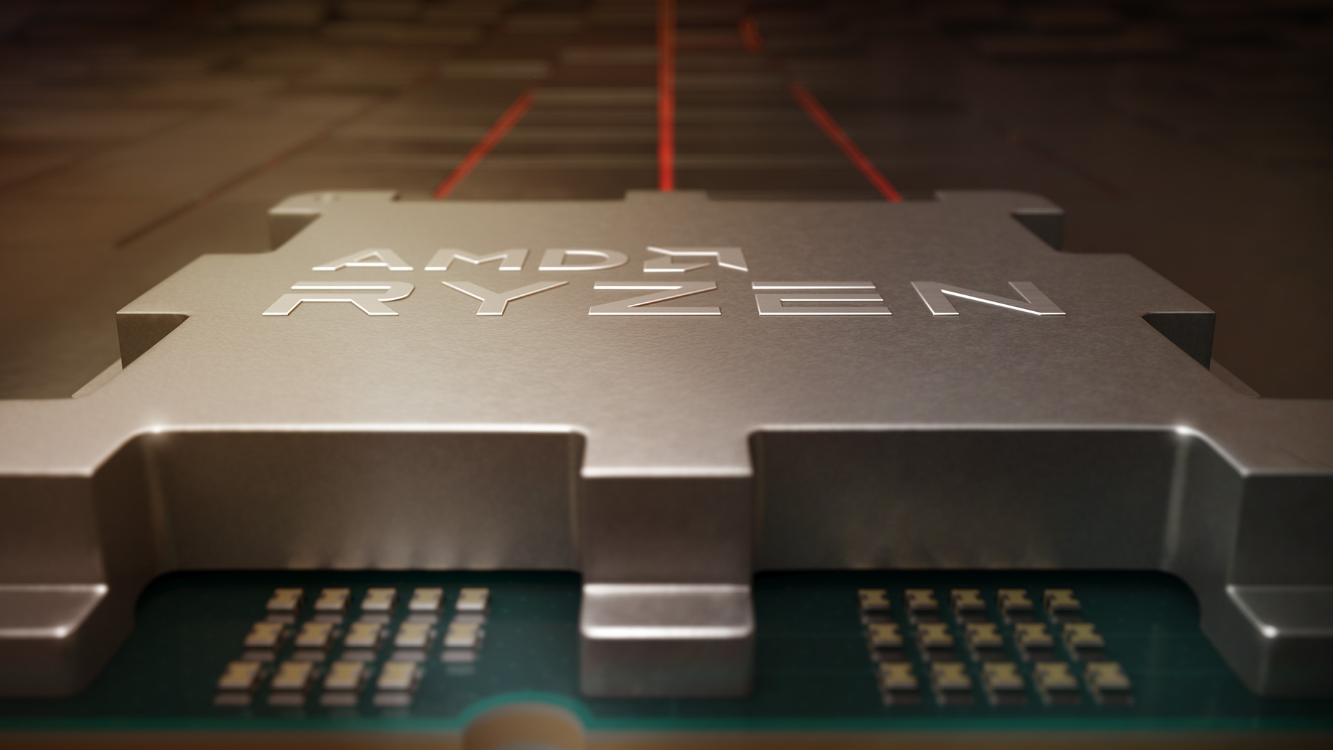
Since then, AMD has filled out the range with cheaper non-X CPUs, such as the 12-core Ryzen 9 7900, and also introduced three new chips that feature a huge stack of 3D V-cache and have ‘3DX’ at the end of their model names. We were highly impressed by the 8-core version, as you can read in our full AMD Ryzen 7 7800X3D review – it lacks the clock speed of the other high-end Zen 4 CPUs, but its huge cache makes it a formidable gaming chip.
On the non-3DX chips, clock speeds have accelerated a long way past their Zen 3 counterparts. The 16-core 7950X tops out at a whopping peak single-core clock of 5.7GHz, which makes for a 0.9GHz or 18 percent maximum clock speed increase over the Ryzen 9 5950X. All the other launch CPUs also have decent boost clocks, ranging from 5.3GHz on the Ryzen 5 7600X to 5.6GHz on the Ryzen 9 7900X.
One negative consequence of the general uptick in clock speed and processing power of the 7000 series, however, is an increase in heat and power draw – ideal timing for an energy crisis. The thermal design power (TDP) for the 5000 series topped out at 105W, but the 7950X and 7900X both have TDPs of 170W. You probably won’t need to upgrade your power supply to accommodate these changes, unless your current one is right on the limit already, but as we found in our testing, good-quality cooling will be essential, as these chips run hot.
Countering this increase in maximum TDP, AMD is also introducing an Eco Mode that can be used to limit the CPUs TDP to 105W or even 65W, although obviously this impacts peak performance, with boosted clock speeds dropping to below 5GHz at 105W and to under 4GHz at 65W in our testing. Nevertheless, we found that we could still get fantastic performance from our Ryzen 7 7700X test chip with Eco mode enabled, as you can see in our guide on how to overclock an AMD Ryzen 7000 CPU.
What will need an upgrade if you want to buy one of these CPUs is your motherboard, as the new chips use a new socket. Out is the pin grid array (PGA) socket of AM4 – where the pins are on the CPU – and in is a land grid array (LGA) layout where the motherboard plays host to the pins and the CPU has flat gold contact points.
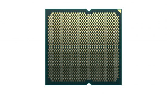
Essentially, it’s shifting the burden of busted pins from the CPU to the motherboard manufacturer, but also allows for a denser grid of pins, with AM5 supporting 1,718 contacts, up from the 1,331 contacts of AM4. You can read our guide to the best AMD X670E motherboard to find your best options at a range of prices. We also recommend using a thermal paste guard when it comes to installing your AMD Zen 4 CPU.
Making your Ryzen 7000-series upgrade even more pricey is the need to invest in DDR5 memory, as Ryzen 7000-series CPUs and AM5 motherboards won’t have support for DDR4 memory at all. DDR5 comes with clock speed and power consumption benefits, but still demands a premium over DDR4. If you’re looking to buy some DDR5 memory, make sure you check out our full guide to the best gaming memory, where we cover your best options at a range of prices.
Finally, one other interesting feature bonus with Ryzen 7000-series processors is that they all include integrated Radeon graphics, which is a first for standard Ryzen chips. Assuming you’re not into gaming, so don’t require the extra grunt of a dedicated graphics card, the integrated graphics here will easily be sufficient for desktop work, saving you on the cost of an extra card.
AMD Zen 4 under the hood
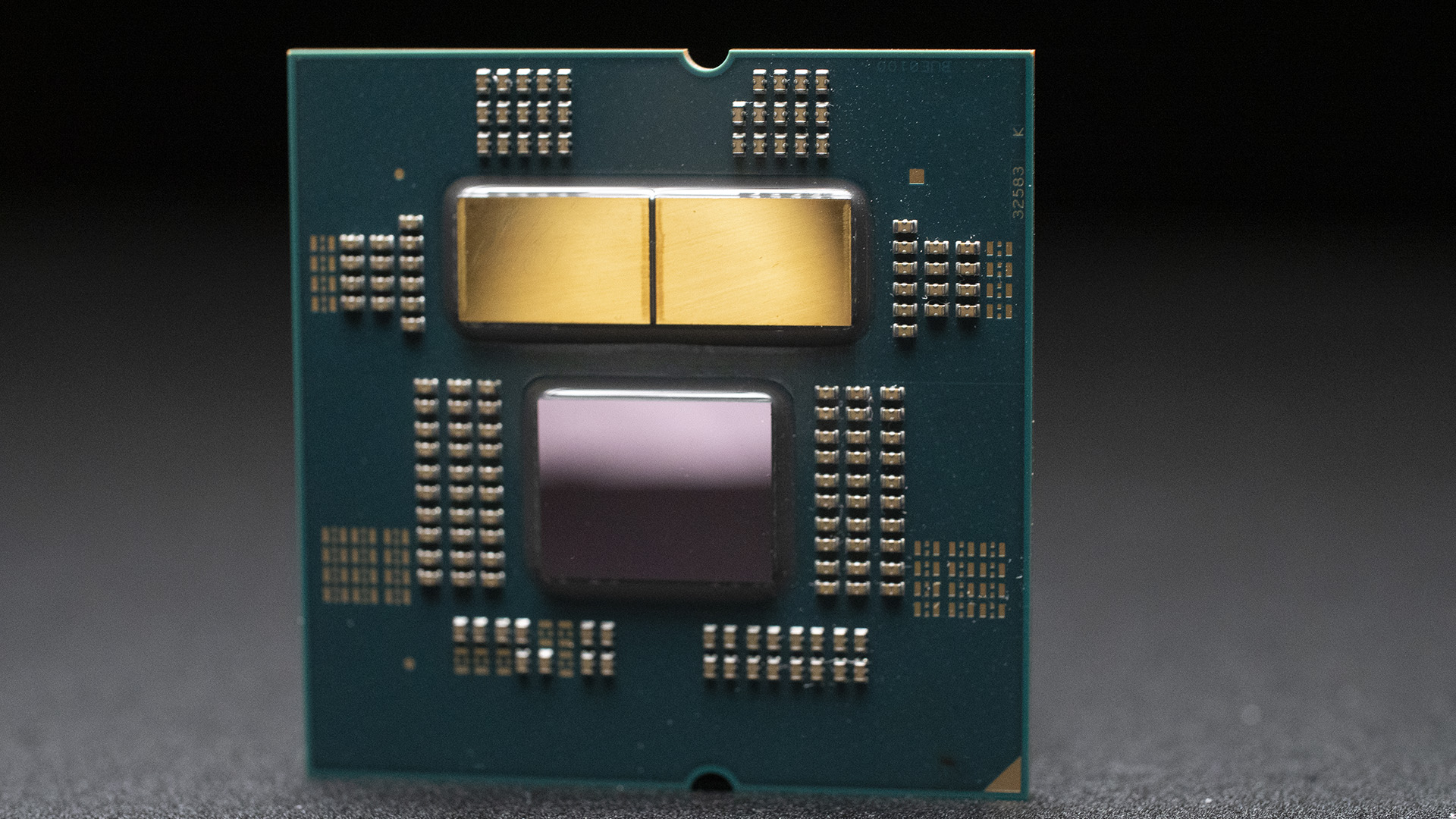
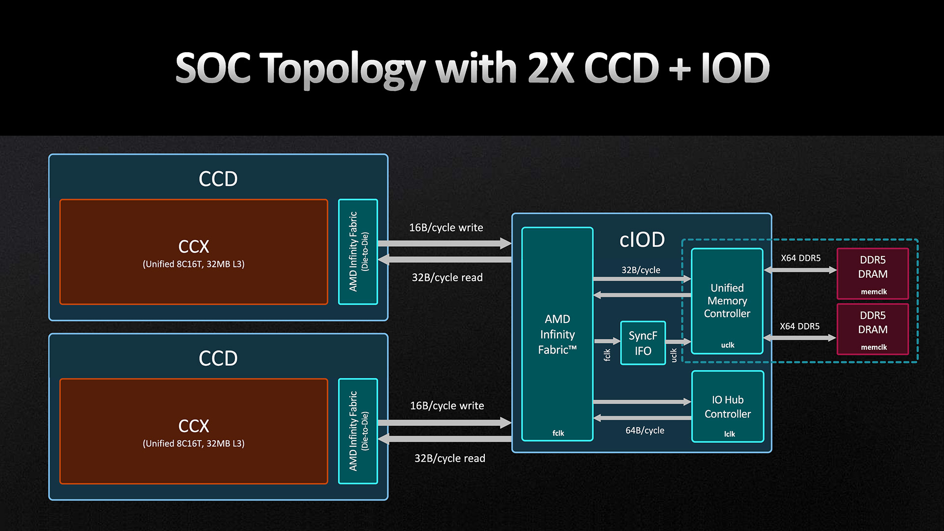
Prise off the integrated heatspreader (IHS) of a Ryzen 7000-series chip and you’ll see two or three main chips, consisting of one or two Zen 4 core complex (CCX) dies (CCD) and the input/output die (IOD).
The IOD controls communication between the core dies, and between the whole CPU and the rest of your system. It includes features such as the Infinity Fabric interconnect, DDR5 DRAM controller, PCIe 5 interface, USB 3.2 interface and more. It’s also where the new RDNA 2 integrated GPU is housed.
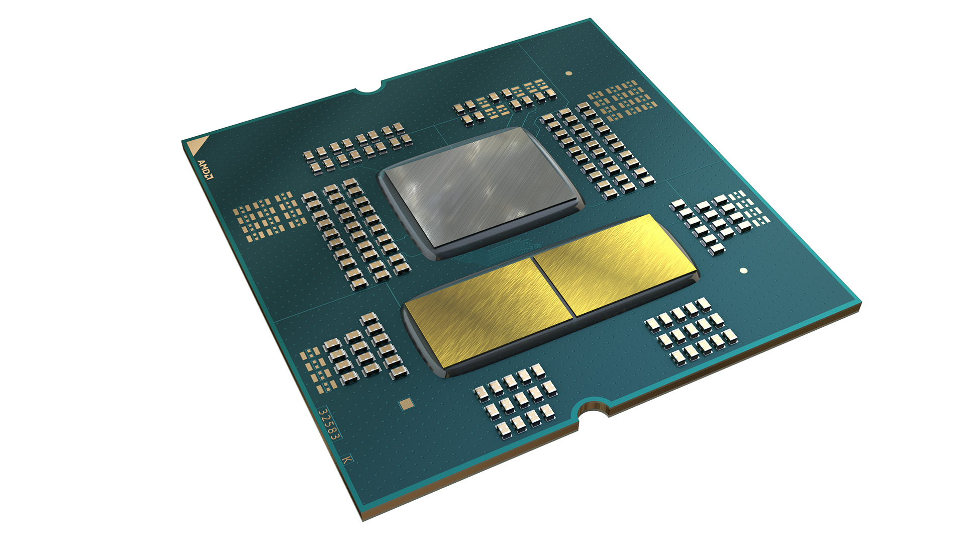
Meanwhile, the CCDs each house eight Zen 4 cores, although only some may be enabled, and you’ll get one or two CCDs depending on the core count of the chip. So, for instance, a Ryzen 7 7770X will have two CCDs with each of those CCDs having two of its cores disabled.
Alongside the cores, each CCD is also home to 32 1MB chunks of L3 cache that are combined – along with the cache from the second CCD – to form a single shared L3 cache for the whole CPU. When cores of a CCD are disabled, the neighboring two 1MB chunks of L3 cache are disabled too.
Aside from an area for the Infinity Fabric interconnect, and a few extra system management units, that’s all that makes up a CCD – all the rest of the CPU’s features are offloaded to the IOD.
This approach of using multiple dies for different functions – known as chiplet design – comes with a multitude of advantages and one main disadvantage. The advantages include improving manufacturing efficiency and cost, as you can fit more smaller CCD dies in a silicon wafer than a larger single die that incorporates everything in the CPU.
You can also do what AMD has done here and use a cheaper, older process for some parts of the CPU, saving the most advanced and expensive processes for just the cores. The impact of any defects is reduced as well, as one ruined CCD uses much less silicon than a whole ruined CPU die.
Other advantages include the ability to create a wide array of CPU designs using the same core building blocks. With the same components, AMD can in theory offer any design from a 2-core to a 16-core desktop processor, and the company’s EPYC server processors use up to 12 CCDs per CPU.
The main disadvantage of chiplet design is managing the data flow between the CCDs and the IOD. Traditionally, resorting to off-silicon interconnects results in significant reductions in speed, but AMD has managed to make its Infinity Fabric interconnect work well enough for its chiplet design to keep up so far.
Intel hasn’t used a chiplet design for its CPUs yet. Instead, it currently uses a single slab of silicon for its 13th-gen Raptor Lake processors, such as the Intel Core i9-13900K. However, it’s set to adopt a chiplet design for its Meteor Lake CPUs in the future.
AMD’s CCDs are built on the latest 5nm process from Taiwan Semiconductor (TSMC) but the new IOD is built on the slightly older 6nm TSMC process. Both are upgrades over the Ryzen 5000 series, which used 6nm or 7nm processes for the core dies and 14nm for the IOD.
As ever, a move to a smaller manufacturing process means a lower power draw and, in this instance, a fairly significant uptick in clock speed too. AMD is claiming Ryzen 7000-series CPUs will provide a 62 percent drop in power consumption for the same performance level as Ryzen 5000-series chips, or a 49 percent uptick in performance for the same power draw.
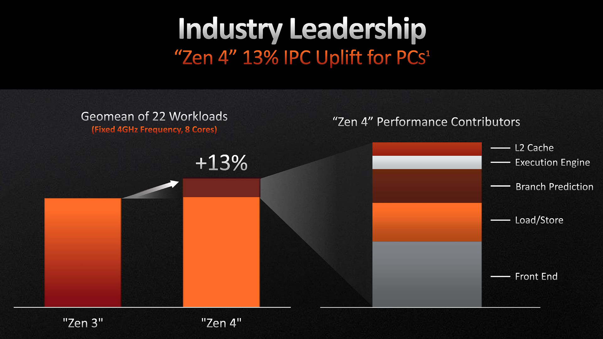
While a lot of that improvement is just down to the new manufacturing process, a significant chunk comes from the new Zen 4 architecture, with AMD boasting a 13 percent uptick in instructions per clock (IPC) over Zen 3.
That’s actually the lowest generational change we’ve yet seen from a new Ryzen processor, but a double-digit uptick is still impressive and, when combined with the significant clock speed gains, AMD expects a step up in single-core performance over Zen 3 of 29 percent.
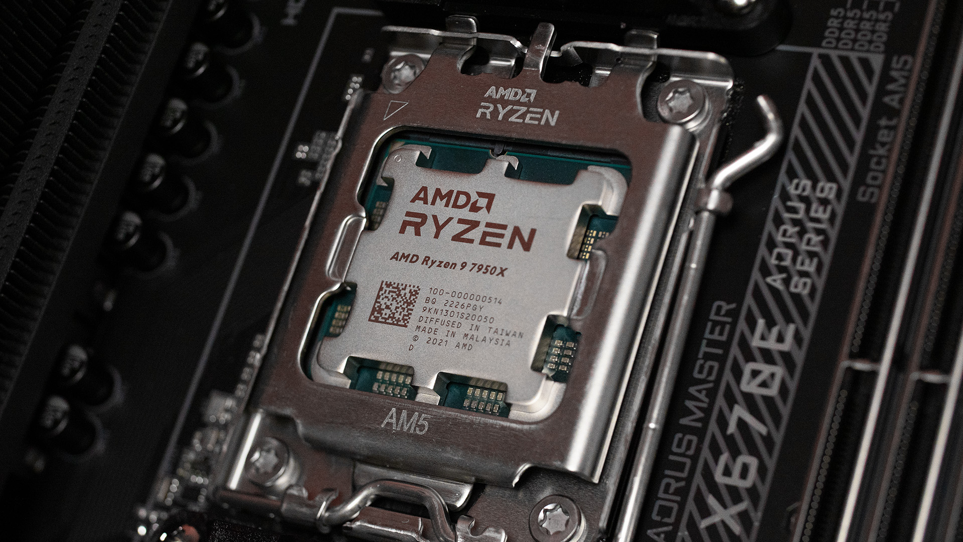
AMD Zen 4 architecture overview
Taking a closer look at the core design of Zen 4, from a block diagram perspective, the overall setup of the new core looks very similar to that of Zen 3, with the same front-end layout, the same execution engine layout and largely the same load/store and cache setup. In comparison, the move from Zen 2 to Zen 3 incorporated several more obvious macro-level changes.
However, on a deeper level, there have been tweaks throughout the design of Zen 4, along with some more obvious changes, such as added support for AVX-512 instructions, a larger L2 cache and a larger micro-op cache. As ever with chip design, it can be the combination of many smaller tweaks that add up to big changes in performance and efficiency, rather than a total redesign being required.
AMD Zen 4 front end changes
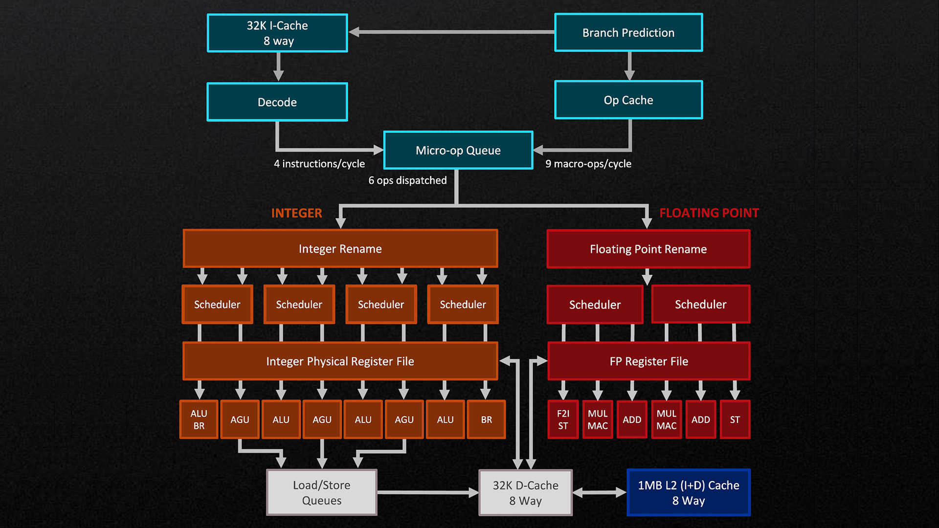
The front end of a processor core design is where larger instructions that have been sent to the CPU are decoded into smaller micro-operations (micro-ops), which are passed on to the execution engine portion of the chip.
These micro-ops are stored in a micro-op queue and then scheduled for execution by the separate integer and floating point portions of the execution engine. Some operations can also be directly passed on to the micro-op queue without needing further decoding, and these macro-ops are stored in the op cache before joining the micro-op queue.
The design of Zen 4’s front end is largely very similar to that of Zen 3, with a 32KB instruction cache that can commit four instructions per clock cycle from its decoder to the micro-op queue, while the macro-op cache can commit up to nine macro-ops per cycle. Zen 4 also retains the six micro-ops per clock cycle dispatch rate of Zen 3 – it can pass six operations per cycle to the integer or floating point engines.
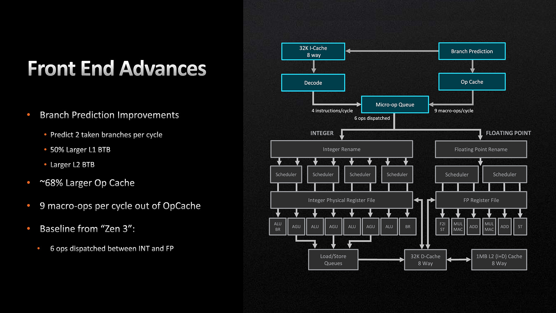
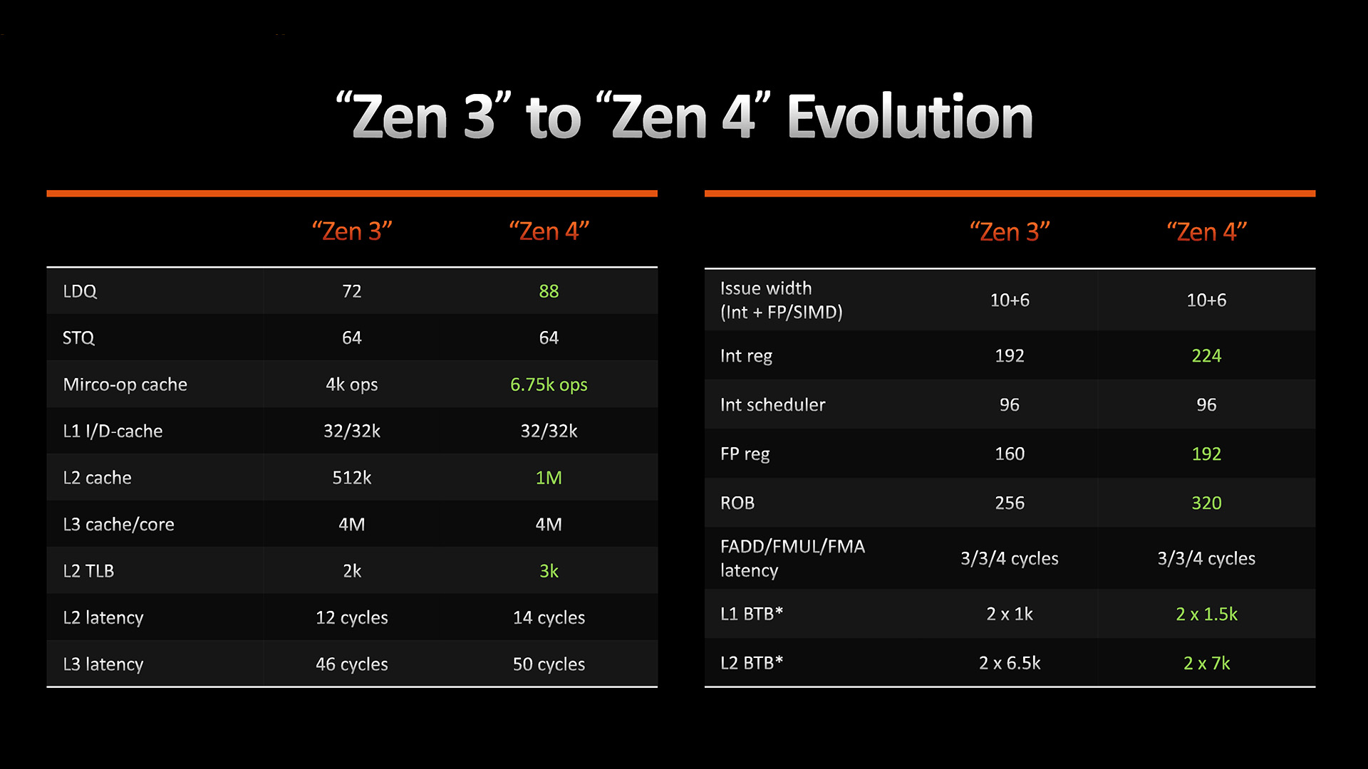
The first big front-end improvement with Zen 4 is a 68 percent larger op cache. This allows the core to handle and prioritize more potential work for the execution engine at once, to ensure it’s passing on work to the execution engine in the most efficient manner.
The branch prediction engine has also been improved. Branching is where a program is waiting on the result of a calculation with multiple outcomes – an if/then/else type of statement. Waiting for branch outcomes to be resolved before proceeding to the next stage can leave the CPU starved of work. As such, CPUs employ branch prediction to guess the outcome of the branch and set up the data and operations for that branch outcome.
Branch prediction is one of the very first stages through which an instruction goes when it’s received by a CPU, as guessing right as early as possible can save a lot of time and wasted resources. With Zen 4, the branch predictor has seen several improvements, including a larger L1 branch target buffer (BTB) and larger L2 BTB.
While AMD has provided a 13 percent IPC improvement figure for the architecture improvements with Zen 4, it doesn’t break down how much each individual change to the architecture contributes to the total improvement. Its visual representation of these proportions (below), shows the branch prediction changes alone account for the third largest contribution to that IPC increase.
Meanwhile, the other combined front-end changes account for the biggest portion of the total IPC increase. In essence, this shows the importance for performance of efficiently managing the workload of the CPU before that workload is passed onto the number-crunching execution engine portion of the chip.
AMD Zen 4 execution engineering
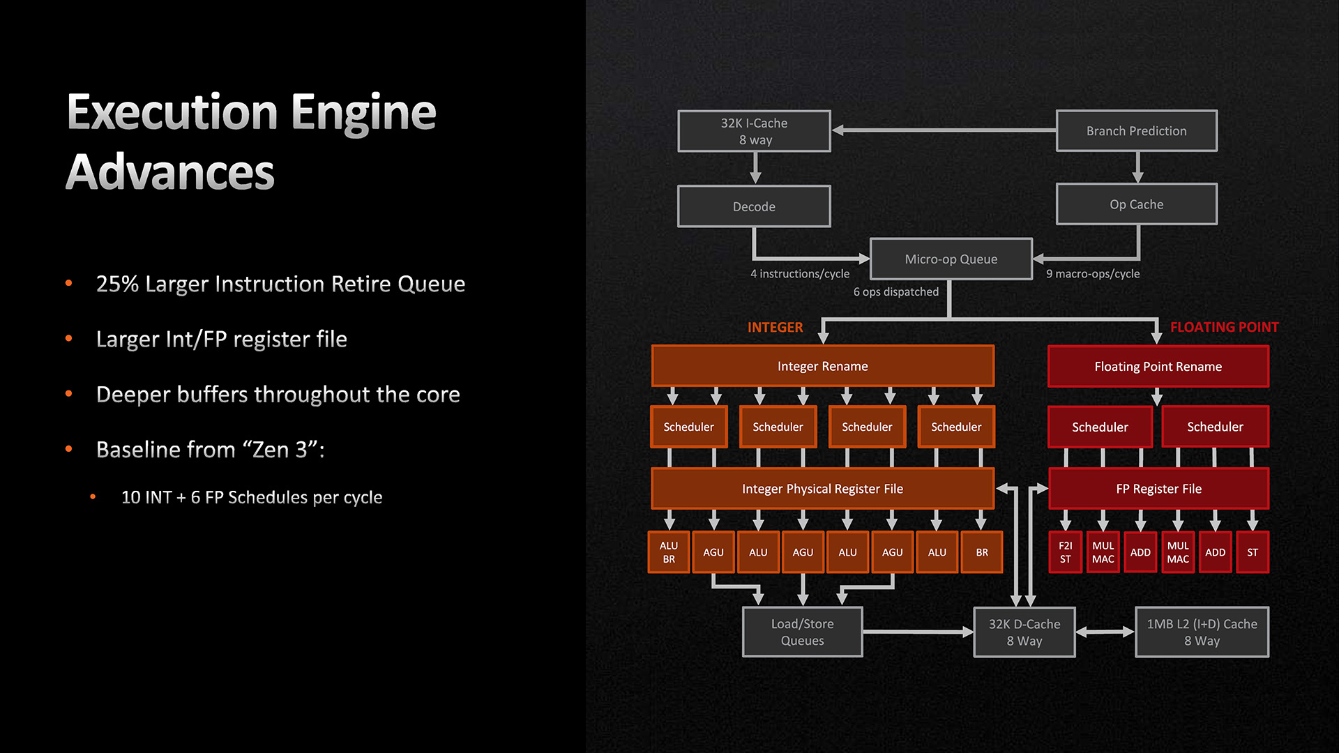
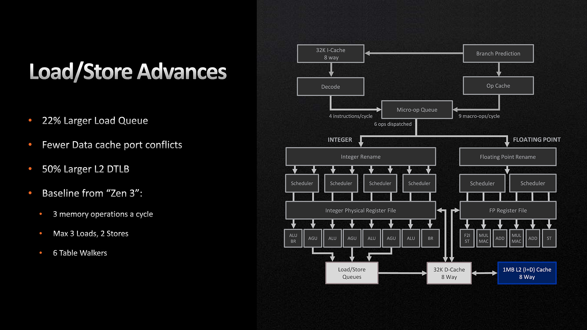
The block diagrams of Zen 3 and Zen 4 show no change between the two when it comes to the execution engine portion of the core – on a macro level, Zen 4’s execution engine is the same as Zen 3. It still has an issue width (the number of operations that can be performed per cycle) of ten for the integer engine and a 6-wide issue for the floating point engine.
The scheduler arrangement also remains the same 4×2 setup for integer and 2×3 for floating point as before. As a side note, a notable difference between Intel’s current core design and AMD’s latest is that Intel uses a combined integer and floating point scheduler, not the separate paths used here.
However, there are changes hidden inside the execution engine that combine to provide a modest uptick in performance. These include a 25 percent larger instruction retire queue, a larger main register file for both integer and floating point engines, and deeper buffers throughout the core. We don’t have any details beyond that, but essentially this adds up to the engine as a whole having slightly larger data stores than Zen 3 throughout.
AMD Zen 4 Load/Store and cache changes
AMD has attributed more of a significant performance uplift to changes to the load and store portions of the Zen 4 core. These deal with moving data back and forth between the core and system memory or internal caches.
Again, the overall setup is largely the same as with Zen 3, with a maximum of three memory operations per clock cycle – three memory loads or two memory stores – and six table walkers (used to automatically manage entries in the translation lookaside buffers). However, the L2 data cache size has been increased by 50 percent, while the load queue has increased by 22 percent as well.
These larger data stores allow more data to be in flight at the same time, increasing the chance that the right data will be available for other operations down the line. The downsides to larger caches are an increase in die space and potential difficulty in ensuring the store can be accessed efficiently, but clearly AMD felt the larger stores would provide a net benefit.
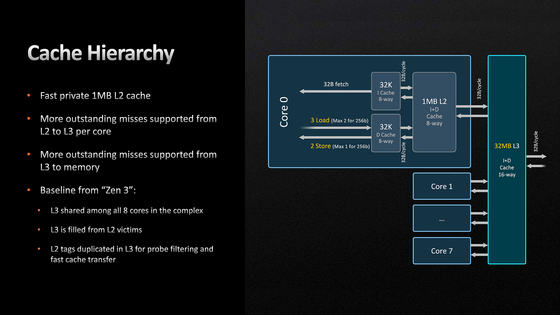
Other changes to the data access structures include support for more outstanding misses from the L2 to L3 caches, and from L3 cache to memory. A cache miss is where the data required isn’t stored in that cache, so the CPU has to move to a higher-level cache, or even to system memory, to retrieve that data.
While those data retrieval processes are being undertaken, the information pertaining to that cache miss is held in what’s known as an outstanding miss store. Increasing the size of these stores ensures that any more cache misses – and the processes associated with them – can be kept on standby, ready to be executed again as quickly as possible when the miss is resolved.
Again, looking at AMD’s visual breakdown of the contribution towards IPC increase provided by each of the changes to the Zen 4 architecture, while the L2 cache change is the smallest block shown, the load/store changes contribute the second largest proportion of improvement. This again shows the importance to processor performance of efficiently managing data in and out of the execution engine.
Zen 4 AVX-512 instructions
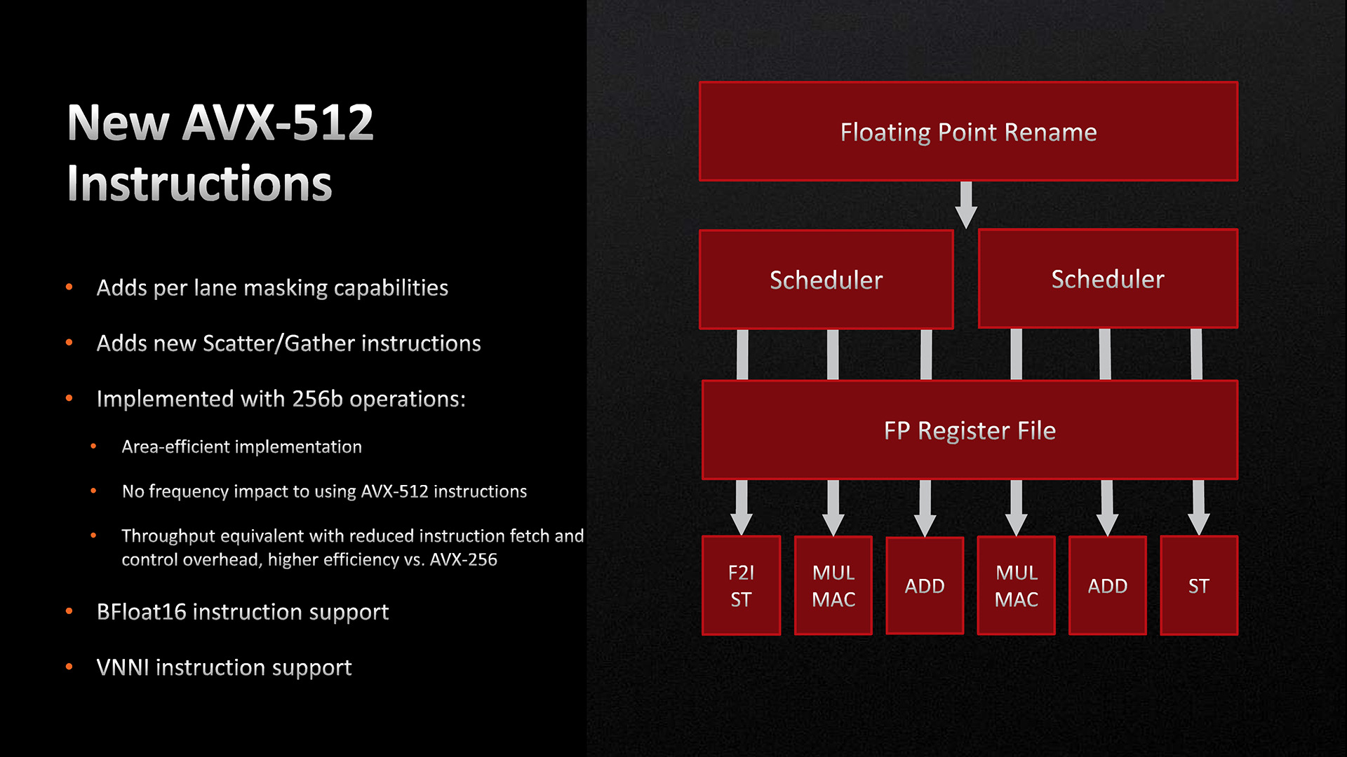
One of the more intriguing additions to Zen 4 is proper hardware support for 512-bit vector instructions (instructions that perform the same calculation on multiple bits of data at once), known as AVX-512. Pioneered by Intel, these are generally only used in scientific, AI and other such specialist applications, but have seen growing support and are a feature that Intel has long highlighted as important.
It’s ironic, then, that with its 12th-gen Core processors, Intel actually removed AVX-512 support. Its removal was in part because of that architecture’s use of different P-Cores (that support AVX-512) and E-Cores (that don’t support AVX-512), which raised complications about managing instructions, but it also pointed to this being a niche instruction set for regular desktop processor users. As such, for AMD to now bring support is particularly notable.
Intel’s AVX-512 implementation was also infamously power-hungry, causing huge power spikes that pushed well beyond the rated power output of the chips. Meanwhile, AMD is claiming power-efficient operation of its AVX-512 hardware. However, AMD’s design uses a 256-bit wide single instruction multiple date (SIMD) design, so it takes two clock cycles to perform a full 512-bit wide instruction, compared with Intel’s full 512-bit wide, single-cycle design, so it’s no wonder AMD can claim its design is more power-efficient.
AMD claims an increase of 1.31x for FP32 inferencing calculations compared with Zen 3, and an increase of 2.47x for Int8 inferencing, thanks to this new AVX-512 hardware.
AMD Zen 4 new IOD
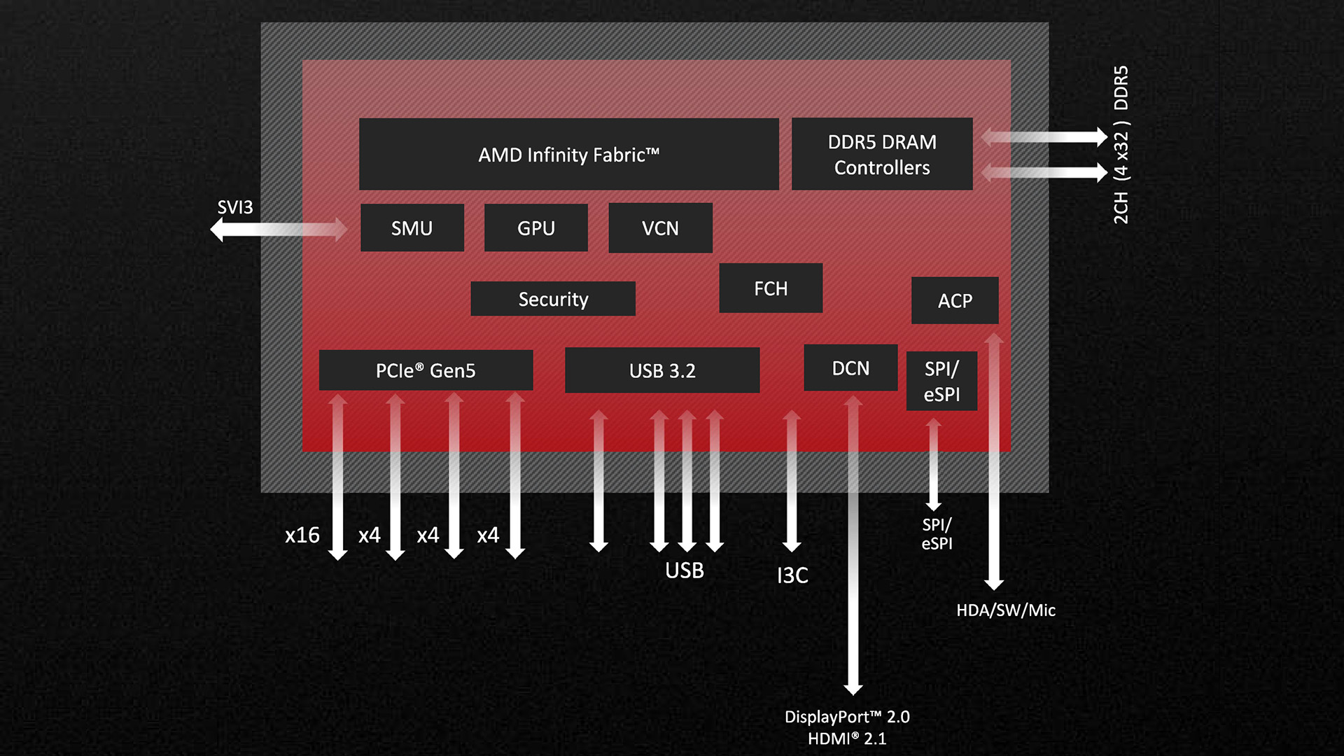
Several of the biggest changes to Zen 4 over Zen 3 pertain to its IOD, as not only does it now incorporate integrated graphics, but it’s also where support for new features such as DDR5 and PCIe 5 come into play. Plus, the whole chip has seen a large change in manufacturing technology, from a relatively ancient 14nm process to a 6nm process.
The net result of this change in silicon manufacturing technology will be significantly lower power draw per on-die component, although with the Zen 4 die being so much denser and feature-packed than the Zen 3 die, it won’t necessarily draw less power overall – it certainly won’t if you’re using the integrated RDNA2 graphics.
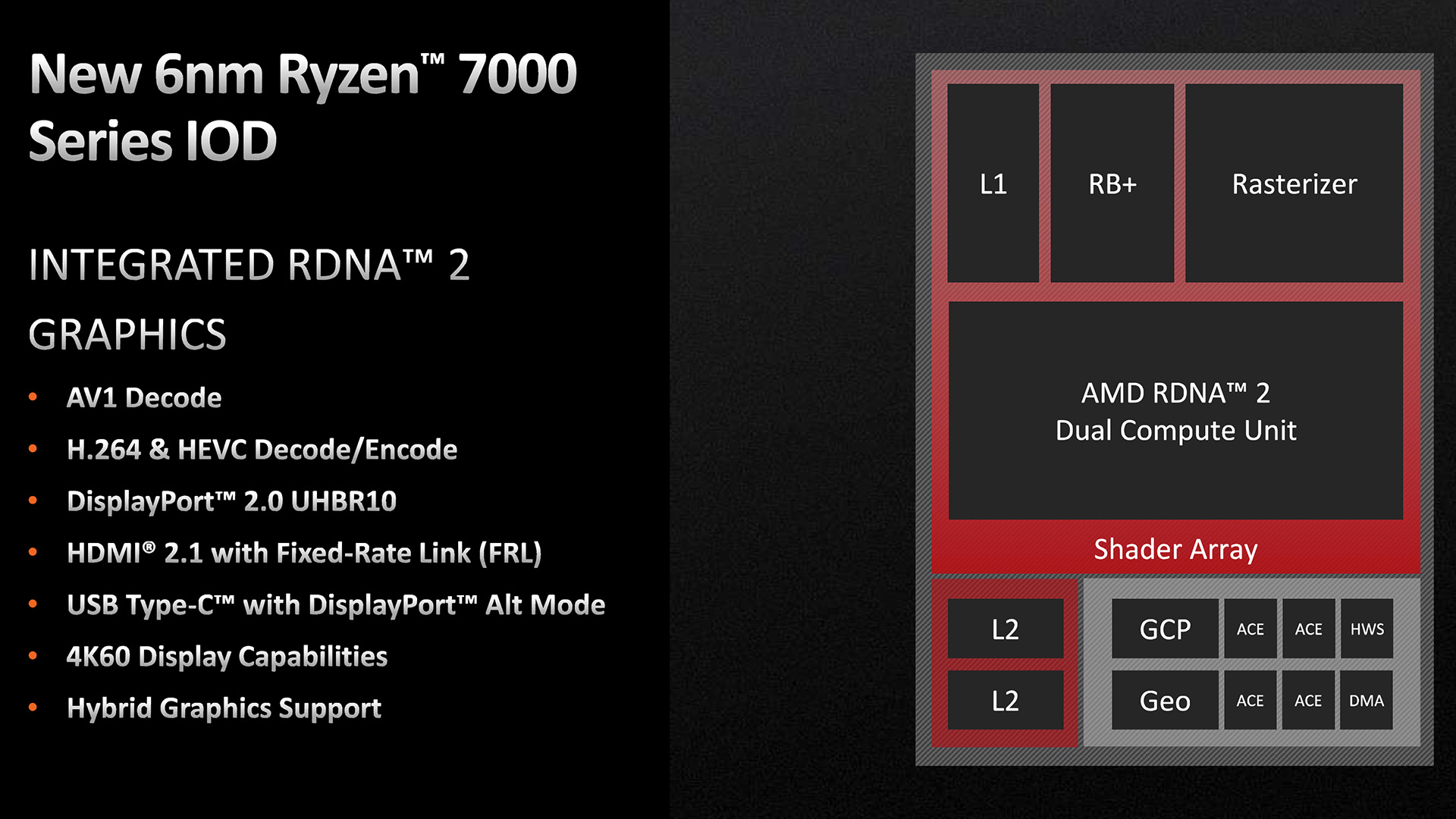
AMD is making it clear that the integrated GPU isn’t meant for gaming, but instead it’s just meant to support desktop usage, with support for high-resolution display output (DisplayPort 2 and HDMI 2.1), USB Type-C with DisplayPort Alt Mode, and AV1 and H.264 video decoding and encoding. This is largely irrelevant for gamers, but for the wider PC market, it opens up AMD’s CPUs to a far greater range of low-cost and compact systems.
What’s more, while AMD says it’s not for gaming as such, the integrated graphics system does still incorporate a single AMD RDNA 2 dual compute unit, so it can technically support all the latest processing requirements to run the latest games, but the emphasis here is on ‘technically’.
RDNA 2 GPUs have 64 stream processors per compute unit, so you’ll get 128 in a Zen 4 CPU’s integrated GPU. Comparatively, a Radeon RX 6600 has 28 compute units (1,792 stream processors), so there’s a huge performance gulf between this integrated GPU and even a modest discrete GPU.
Socket AM5 and new motherboard chipsets
The final piece of the Ryzen 7000-series platform puzzle is the launch of AMD’s accompanying new AM5 socket and a raft of new motherboard chipsets, as well as all the related motherboards, to support the new processors.
Along with its higher pin count and flipped pin arrangement, Socket AM5 also includes several power-related enhancements, including two-way communication to motherboard voltage regulators and voltage regulator health monitoring. The result should be better system stability and potentially more overclocking headroom.
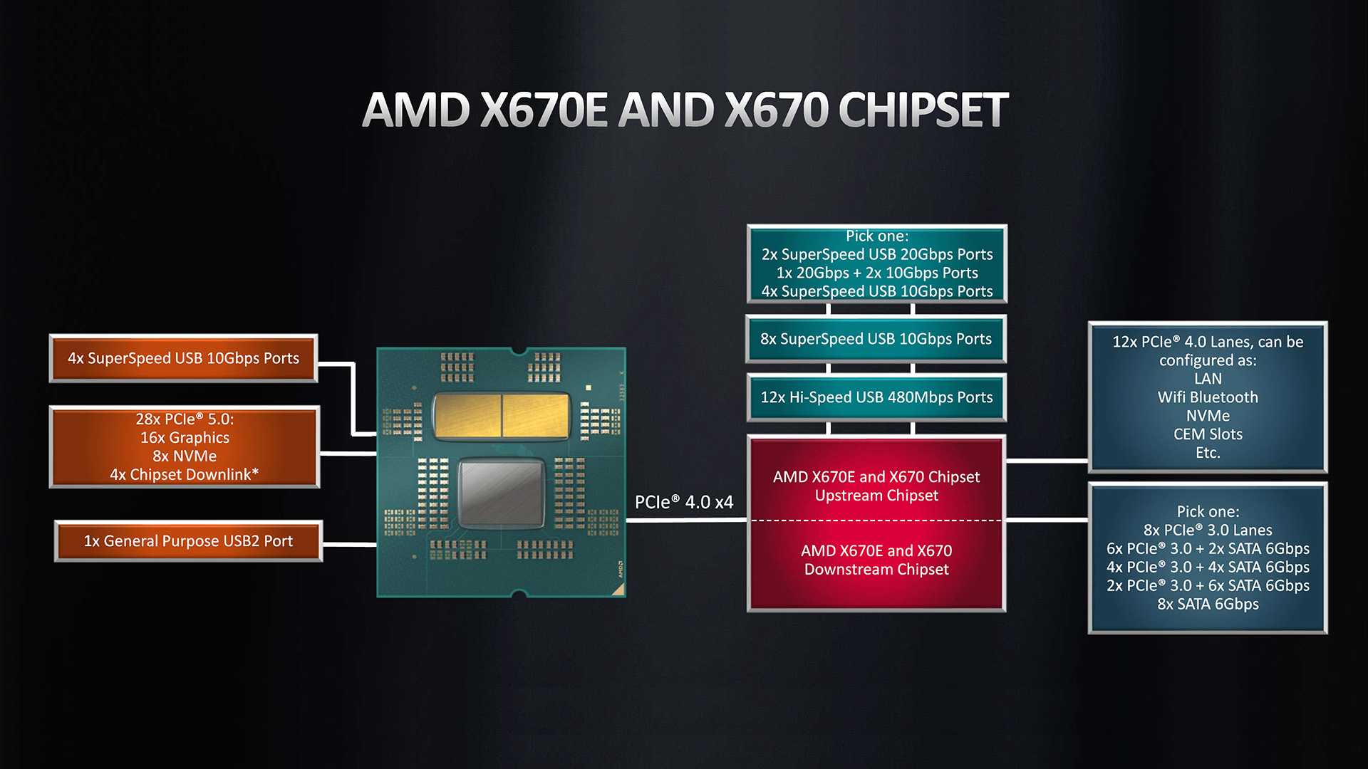
As for those chipsets, AMD offers four of them: the X670E, X670, B650E and B650. However, while AMD talks about chipsets, in reality, the company has only created one chipset die that will be implemented in different configurations for each chipset type.
As such, for X670 and X670E motherboards, two dies will be used in an uplink and downlink configuration, while the B650 variants will use a single die for both.
The upshot is that X670-series boards will provide essentially double the features and connection options of B650-series boards. So, for instance, you’ll get two SuperSpeed USB 20Gbps ports and 12 USB 480Mbps ports on an X670 board, compared to one SuperSpeed USB 20Gbps port and six USB 480Mbps ports for B650, unless the motherboard maker adds third-party controllers.
Other differences between the chipsets include X670E configurations supporting PCIe 5 across all PCIe slots and M.2 slots, whereas X670 only supports it for one PCIe slot – the rest will be PCIe 4. Meanwhile, B650 has fewer connection options than the other chipsets, and A620 has even fewer, while also not allowing overclocking support.
AMD EXPO memory
Launching alongside Zen 4 is AMD’s new EXPO memory technology. Fundamentally a rival to Intel’s eXtreme Memory Profiles (XMP), EXPO is AMD’s one-click technology for overclocking DDR5 RAM.
Like XMP, EXPO-certified memory will guarantee stable performance of a memory kit for the EXPO-rated clock speed, voltage and timings. Also, like XMP, it doesn’t necessarily guarantee that the kit will play ball with your chosen CPU at its rated speed – just that the memory kit can reach those speeds in isolation.
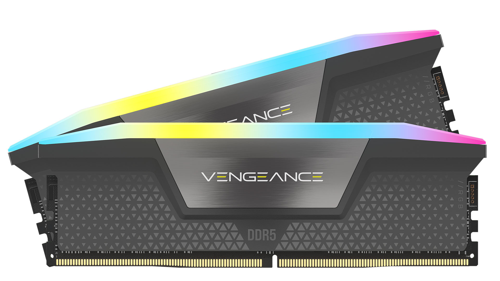
However, given the kits will have been tested with AMD CPUs – rather than with Intel CPUs, as is the case for XMP – you stand a greater chance of it working with your new AMD chip than a non-certified memory kit. We found EXPO worked well in our tests, which you can see for yourself in our AMD EXPO memory benchmarks feature. We’ve also recently reviewed some Corsair Vengeance RGB EXPO DDR5 memory kits.
Final thoughts
AMD’s Zen 4 CPUs undoubtedly got off to a shaky start when they were first released at the end of 2022. The motherboards were expensive, as were the new CPUs, and unlike Intel’s 13th-gen and 12th-gen chips, you were also forced to use DDR5 memory. Since then, however, the price of these CPUs has dropped, and the price of DDR5 memory has plummeted.
Meanwhile, the recent introduction of AMD Zen 4 CPUs with 3D V-cache has made AMD the winner when it comes to gaming performance. Intel’s top-end 13th-gen Raptor Lake CPUs are still great for multi-threaded performance, and the Core i5-13600K makes for a great cheap upgrade, as you have the option of using your old DDR 4 RAM.
However, if you’re building a new system from scratch, we thoroughly recommend building an 8-core rig based on the Ryzen 7 7700, or a top-end gaming system based on the Ryzen 7 7800X3D.
We hope you’ve enjoyed taking a deep dive into the AMD Zen 4 CPU architecture with us. If you’re on the lookout for a new CPU, then check out our full guide to the best gaming CPU, where we list several options at a range of prices.
