Packaging your CPU inside a big box before slotting it into your motherboard seems like a recipe for a thermal catastrophe now, but for a brief period around the turn of the Millennium, Intel (and later AMD) mounted their CPUs on circuitboards inside sleek black packages. Meet the Slot 1 design, used on the Intel Pentium II and Pentium III.
They looked great too. There was now room for proper logos and a flashy physical design. Instead of dropping a nondescript-looking ceramic square into your motherboard, you had a fancy black box with a hologram on the front.
With their slick packaging, the first Pentium II CPUs looked great in the TV adverts and promo shots. I remember wanting one just because they looked so good – a small hologram sticker clearly goes a long way toward manipulating people like me! To the uninformed, it looked like these attractive slot-based CPUs were the way of the future, but if you took a peek inside the box, they were clearly a result of technological limitations at the time.
Intel Pentium II L2 cache
To understand the need for slot processors, we need to start by going back a bit further in time. Before the Pentium II, Intel had two major CPU designs. It had the Socket 7 Pentium MMX for consumer PCs, which was the last gasp for the first Pentium design, now running at up to 233MHz.
MMX stands for multimedia extensions, and it effectively enabled a lot more functions to be handled in software on the CPU, rather than in hardware. For example, an MMX CPU enabled you to properly use a software PCI modem, rather than a full hardware one, saving you some money.
For servers and workstations, Intel had also introduced the Pentium Pro, a massive chip that was heavily geared towards pure 32-bit computing. It lacked consumer frills such as MMX instructions, but you could run more than one Pentium Pro in parallel on a multi-socket board.
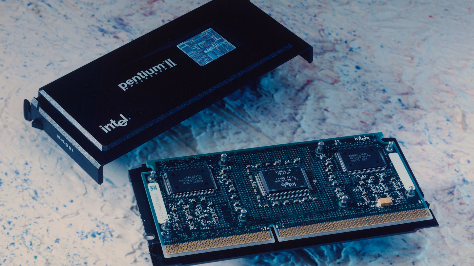
An original SECC Pentium II – look at the size of the cache chips on either side of the CPU area
The Pentium Pro also had a massive L2 cache that ranged between 256KB and 1MB, depending on the model. At this time, there was no way to integrate this cache directly into the CPU die, but the Pentium Pro did incorporate its huge L2 cache in the same Socket 8 package as the CPU die, and it also ran the cache at the same speed as the CPU. There was a big problem with this approach at the time though – making these Socket 8 packages with full-speed cache was an expensive process, and there were low yields.
Intel wanted to combine the two ideas, making a desktop CPU with loads of L2 cache, as well as consumer features such as MMX. It also needed to be better at executing 16-bit code (which was still used by some software at the time) than the Pentium Pro and, most importantly, it needed to be affordable to manufacture on a large scale.
This meant compromising, as Intel knew it couldn’t practically equip a mainstream desktop CPU with loads of full-speed cache in a socket package. The answer was to manufacture the CPU package on a usual square format without the L2 cache, and to then mount that package on a circuitboard that contained the cache, resulting in the Pentium II in 1997. It had 7.5 million transistors, produced on a 350nm manufacturing process.
Like the Pentium Pro, the CPU used a separate ‘back-side bus’ to communicate with the cache, but unlike the Pentium Pro, the Pentium II could only run the L2 cache at half the speed of the CPU. Intel attempted to counter the performance of the cache by first doubling the amount of L1 cache, from the Pentium Pro’s 16KB to 32KB on the Pentium II.
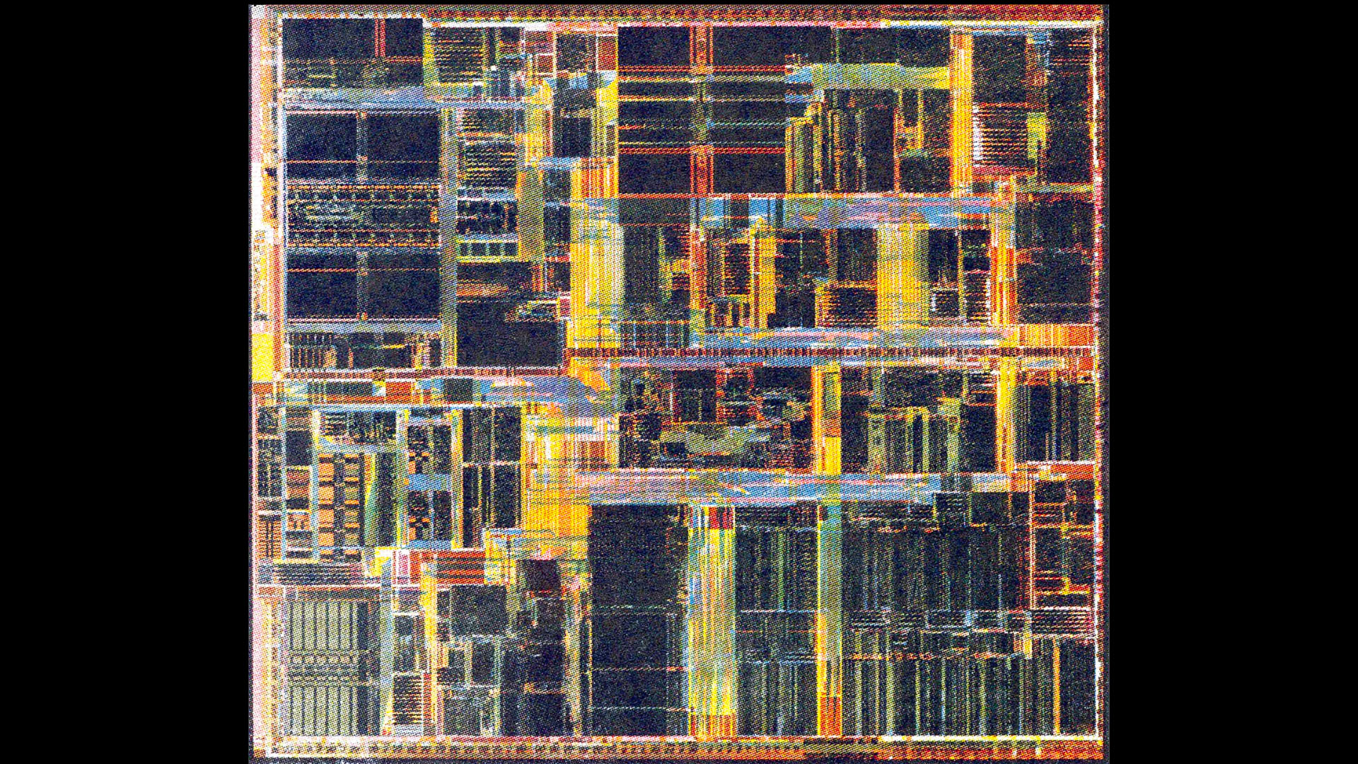
Inside a Pentium II die – that’s 7.5 million transistors produced on a 350nm manufacturing process, and with no integrated L2 cache
The Pentium II’s L2 cache also had a 16-way associativity, compared with 8-way on the Pentium Pro. A higher associativity means the CPU has a greater chance of finding the data it needs in that cache, but that it can take longer to search for it than a cache with lower associativity.
The other way Intel bumped up the Pentium II’s performance was by simply equipping it with a lot of this L2 cache. All the first models of Pentium II came with a pair of large 256KB cache chips, giving you 512KB in total – more than you found on some Pentium Pro CPUs.
By the end of it, you had a circuitboard containing a full CPU package in the middle, with two large cache chips next to it. This was then encased in a box with a thermally conductive metal back. The whole package was called a single-edged contact cartridge, or SECC, and you would then attach a heatsink and fan arrangement to the metal back, and slot the whole setup into your motherboard.
The SECC package looked good on the surface, but if you took one apart, you could see that it was a bit of a bodge job. I was working in a computer shop at the time, and we joked that the Pentium II was a ‘Socket 7 on a circuitboard’ – you could even see the solder points where the socket pins could have been located on the CPU package. It was still a normal square CPU package – it was just mounted on a board instead.
Performance was mixed. If you were running full 32-bit software in Windows 95, then the Pentium II was generally faster than the Pentium MMX, but the latter still had the edge in some 16-bit software, such as MS-DOS games.
It also didn’t help that the first Pentium II CPUs used the same 66MHz front side bus as the final Pentium MMX chips, with the first Pentium IIs running at 233MHz, 266MHz and 300MHz, and a 333MHz variant arriving later, following a die shrink to 250nm. This meant that, in some cases, the top-end 233MHz Pentium MMX was faster than the low-end 233MHz Pentium II.
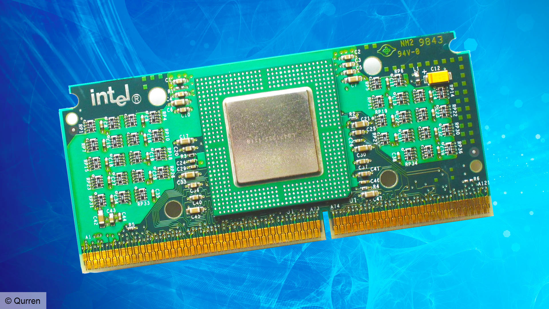
Slot 1 Celerons didn’t come in a fancy chassis, and the first models didn’t come with any L2 cache either.
Intel Slot 1 Celeron
The processor’s new clothes came well and truly off in 1998 when Intel introduced its budget range of Slot 1 CPUs, with the still ridiculous name of Celeron. The first generation of Celeron CPUs, codenamed Covington, removed all of the L2 cache from the circuitboard, as well as all the fancy, hologram-clad packaging. This left you with a peculiar-looking green circuitboard with a square CPU clearly soldered into the middle of it – Intel called this non-cartridge arrangement a SEPP format.
The lack of cache meant these Celerons performed poorly at the time, pushing people looking for a budget CPU towards the AMD K6 line-up, which still used the aging Socket 7 form factor that Intel had deserted. However, the next generation of Celerons in 1999, codenamed Mendocino, overturned this part of CPU market. They were still mounted on circuitboards at first, but Intel had now nailed a method to produce a small amount of L2 cache on the same die as the CPU, running at full speed.
These new Celerons came with 128KB of full-speed on-die cache, meaning they were quicker than the 1st-gen (and much more expensive) Pentium II CPUs in some applications. By this time, Intel’s next generation of Pentium II CPUs used a 100MHz front side bus, rather than 66MHz, which provided a significant performance boost over their predecessors.
Accompanied by the new Intel 440BX chipset, the new CPUs ran at 350MHz, 400MHz and 450MHz, and Intel clearly hoped that this FSB tweak would help distinguish the Pentium II line-up from the new Celeron lineup, despite the latter’s faster cache.
Unfortunately for Intel, overclockers had started discovering that there was plenty of headroom for some of the Mendocino Celerons to go much faster, despite Intel locking down the multipliers in an attempt to prevent it. If you put a new Celeron in an Intel 440BX board, or a board with VIA’s competing 100MHz FSB Apollo Pro chipset, you could try moving the 66MHz FSB jumper to the 100MHz setting.
If you were lucky, and you had a decent heatsink and fan on your CPU, your 300MHz Celeron would suddenly be running at 450MHz, thanks to its 4.5x multiplier. Combine the clock speed with the full-speed cache and your $60 processor could potentially outperform a $400 one.
I remember this well, and bought a 333MHz Mendocino Celeron with a 5x multiplier, in the hope of running it at 500MHz. It booted, but soon fell over once you got into Windows. Thankfully, my VIA Apollo Pro board also gave me the option to run the FSB at 75MHz or 83MHz if you tweaked the jumper switches right, and the latter setting stably ran my budget CPU at 415MHz. I had no need to buy a Pentium II now.
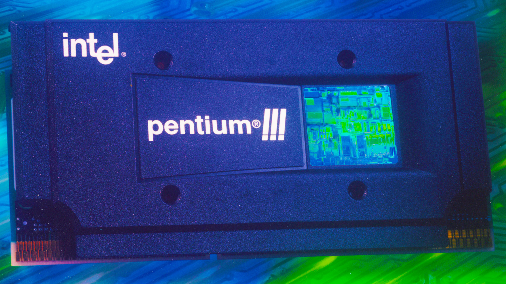
The Pentium III maintained the front with the hologram, but used the new SECC2 packaging, which left the circuitboard bare at the back
Intel Slot 1 Pentium III
While the first Mendocino Celerons were still mounted on Slot 1 circuitboards in order to maintain motherboard compatibility, their L2 integrated cache design meant they no longer technically needed the rest of the circuitboard. A few months later, the first Socket 370 Celerons started appearing, with ‘Slotket’ adaptors required in order to plug them into Slot 1 motherboards. It was a bizarre setup that persisted for an unusual length of time.
Intel wasn’t quite ready to give up Slot 1 yet. Intel started by tweaking the design of the CPU chassis, removing the metal plate at the back. The final arrangement, called SECC2, retained the plastic front cover with the hologram but left the circuitboard and CPU die bare at the back, in order to facilitate better thermal transfer to the cooler.
Next came the Pentium III, codenamed Katmai, which added SSE instructions, but was still fundamentally based on the same P6 core as the Pentium II. It also still had an external half-speed L2 cache setup, with both the CPU and cache mounted on a circuitboard. It wasn’t until the Coppermine (don’t be fooled by the name – all the interconnects were aluminum, rather than copper) revision of Pentium III, with a die shrink to 180m, that Intel finally integrated 256KB of full-speed L2 cache into a CPU die containing 29 million transistors.
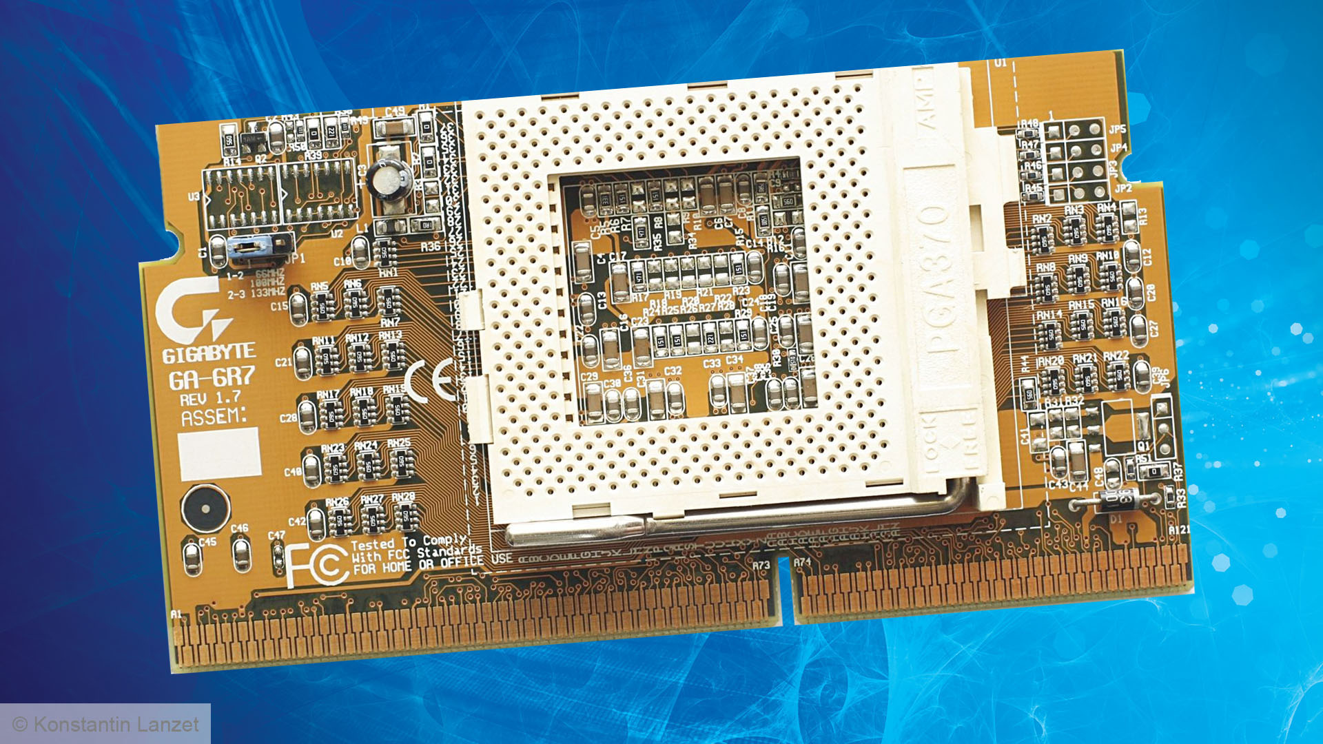
‘Slotket’ adaptors enabled you to plug a Socket 370 CPU into a Slot 1 motherboard
Later came a 133MHz front side bus and Intel’s 820 chipset, accompanied by high-bandwidth but expensive RDRAM. However, the Slot 1 design still persisted. Even the first Pentium III to break the 1GHz barrier was based on a slot design. Intel needed to maintain compatibility, which was handy for many of us enthusiasts who had worked out that you could still run the latest CPUs on some old 440BX boards by overclocking the front side bus to 133MHz. There was also no shortage of Slotket adaptors at this time, enabling you to install Socket 370 CPUs into Slot 1 motherboards.
The final Slot 1 CPU I saw was an engineering sample of a 1.13GHz CPU, but the chip was recalled due to stability problems. The slot era was now over, and motherboards based on Intel’s later SDRAM-based 815 chipset only came in Socket 370 format.
The Pentium III carried in on socket format, as did the later Pentium 4, and the CPU industry hasn’t looked back since. Slot processors might have looked good, and a part of me misses the fancy casing with the holograms, but there’s no doubt that integrating cache directly onto the die is a much faster and more efficient way of doing it.
Of course, CPUs have since changed again since the pin and socket design, with both Intel Raptor Lake CPUs, and AMD Zen 4 CPUs, now using an LGA socket. If you’re looking to buy a new processor, then make sure you check out our guide to the best gaming CPU, where we take you through all the best options at a range of prices. One of our favorites from Intel’s current lineup is the Intel Core i5-13600K, which is cheap, fast, and also overclockable.
We hope you’ve enjoyed this personal retrospective about the era of Slot 1 CPUs. For more articles about the PC’s vintage history, check out our Retro tech page, as well as our full guide on how to build a retro gaming PC.
