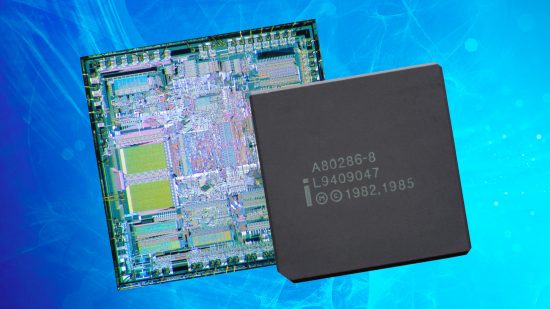
We’re now so used to tiny transistors that the 5nm process used to fabricate the latest AMD Zen 4 CPUs hardly seems worth mentioning now. It’s hard to keep track of the numbers of transistors when they get into billions. However, you only have to look at early PC CPUs to see just how far silicon manufacturing has come. The Intel 286 processor (or the 80286, to use its full title) was released in 1982, and fabricated on a 1.5µ (1,500nm) manufacturing process
Compare that to the 3µ (3,000nm) process used by its predecessor, the Intel 8086. The 286 packed in 134,000 transistors: 4.6 times as many as the 8086. Fast forward to today, and the AMD Ryzen 9 7950X contains over 13 billion transistors. We’ve come a long way.
Clock speeds have rocketed over the decades too. The 80286 was introduced with an entry-level-model clock speed of just 6MHz. This figure would go as high as 12.5MHz for the popular Intel 80286-12, and up to 25MHz for late-era takes on the CPU by other manufacturers, such as AMD and Harris. It would be the last, fastest 16-bit PC processor Intel made.
Its successor, the 80386, was a true 32-bit processor, with a 32-bit data bus and memory addressing to match. However, even as its technology was superseded, the 286 was just hitting its stride in the home PC market, which it would dominate until 386 and 486-based PCs started to become vaguely affordable in the early 1990s.
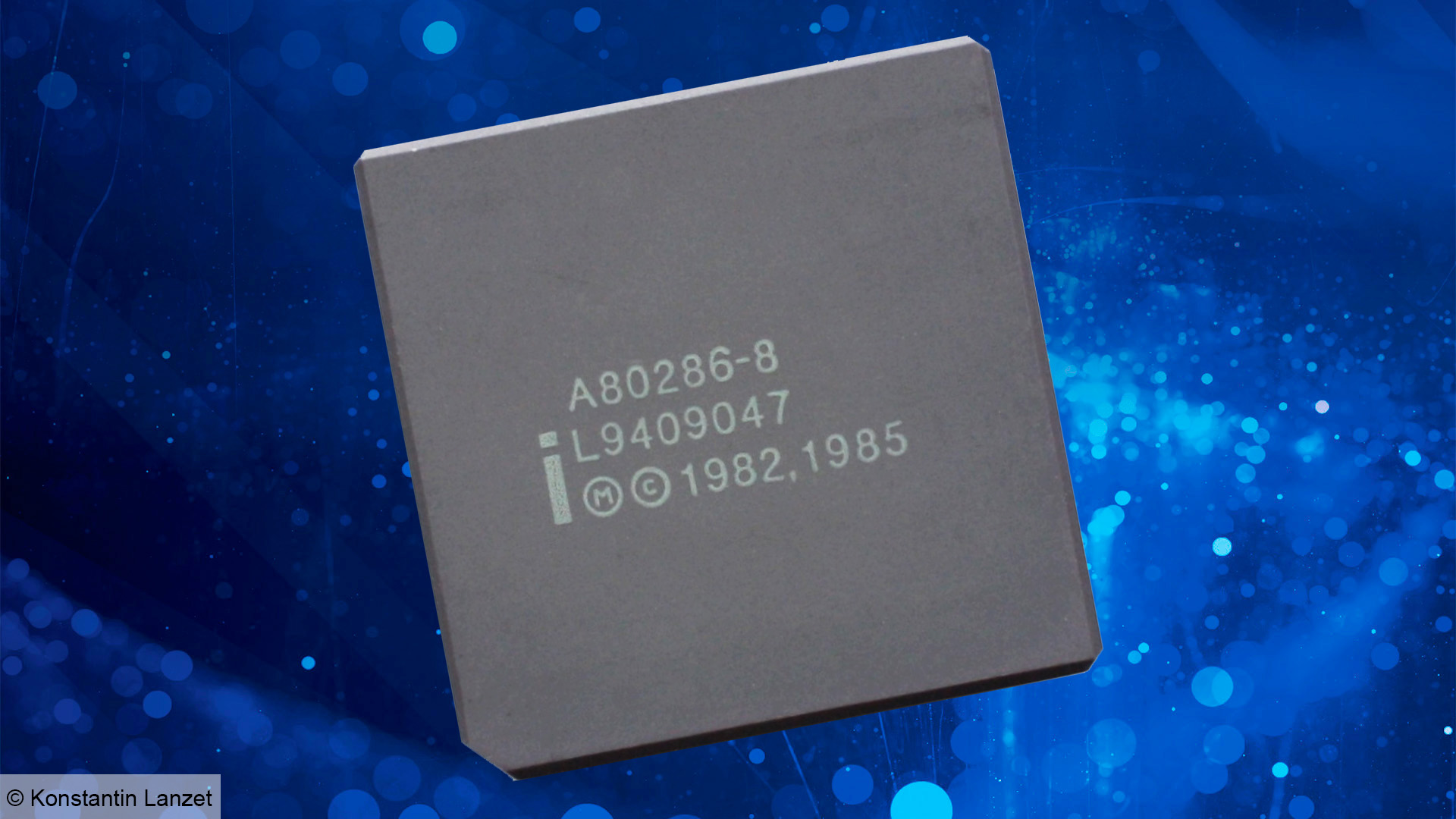
Intel 286 – a vision for the future
When development began on the 80286 in 1979, Intel’s product requirements document envisioned that the powerful new processor would be primarily used in industrial applications, from telecoms to manufacturing automation and medical instruments.
It was explicitly designed to be compatible with the 8086, ensuring that software for the older processor would run without modification on the new device. However, unlike the 80186, PCs weren’t on the 286’s original roadmap.
In Intel’s 1984 annual report, which details the 286’s development, release, and nascent domination of the industry, the company admits that in hundreds of pages of planning materials ‘the personal computer – which would eventually become its biggest user – wasn’t mentioned once’.
The 80286 was announced in February 1982, and the designers had a working prototype to show industry partners that spring, promising ‘about three times the performance of any other 16-bit microprocessor’. However, after initial testing of the first 286 wafers, ‘progress just seemed to drop to a snail’s pace’, according to logic design supervisor Jim Slager, again quoted in Intel’s 1984 annual report. The processor wasn’t yet running fast enough, and the testing programme for CPUs that would come off the manufacturing line was running late.
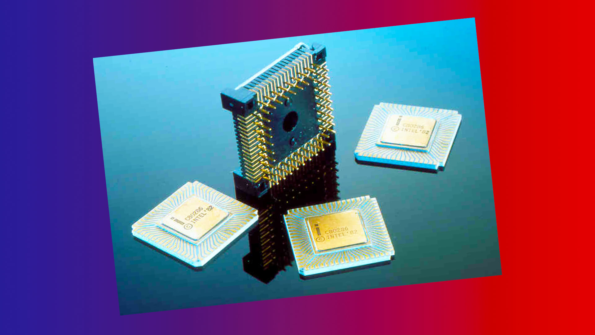
But in June 1982, IBM – then the world’s largest maker of computers – came calling. IBM had been using Intel’s 8088 since 1979 and it was looking to give a power boost to its next generation of PCs: the IBM model 5170, better known as the IBM PC/AT. This came after the IBM XT, which in turn came after the IBM PC 5150.
Intel pulled together a cross-disciplinary task force to complete the testing tools, address bugs, and complete the parallel development of motherboard components. Marketing focused on a new public presentation of the 80286, highlighting its superiority to Motorola’s popular 68000 processor and emphasizing that it was far more than a minor update to the 8086.
Intel emphasized the 286’s multi-user and multi-tasking capabilities, including variable privilege levels to restrict access to specific parts of memory, as well as an instruction set designed to rapidly switch between programs, providing support for Unix as well as DOS.
The marketing push – and especially IBM’s adoption of the processor – worked. Chip samples were delivered to customers later the same year and, in 1983, volume production of the 80286 began. The IBM PC/AT launched in August 1984, prompting a wave of AT-compatible computers from companies including Compaq and NEC. By the end of 1988, Intel estimates there were around 15 million 286-based PCs in use worldwide.
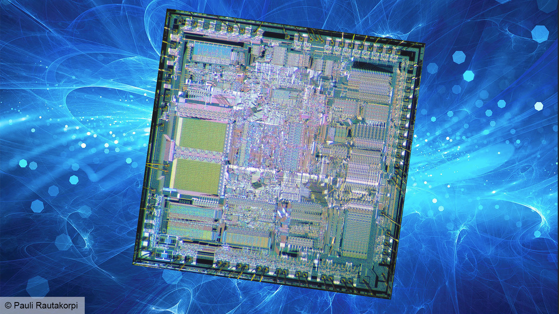
Intel 286 memory bus
Changes to memory handling were a headline feature of the 286, but software support was slow to emerge. The processor introduced protected mode memory addressing and retained real mode addressing to ensure compatibility with applications designed for the 80186, 8088, and 8086.
In real mode, like the 8086, the 286 can address up to 1MB of memory via a 16-bit address bus. In protected mode, it can address up to 16MB of memory using a 24-bit bus. This approach has security and stability benefits in that, in protected mode, different programs and users can’t access memory segments in use by others.
Protected mode made the 286 compatible with Unix-based operating systems such as Microsoft Xenix, and its secure memory handling made it possible for up to eight users on terminals to be connected to a 286-based Xenix server.
To ensure backward compatibility, the system has to boot in real mode and then be switched into protected mode by setting a status register bit. To get out of protected mode, you have to reset the CPU. This switching process was crash-prone in some versions of the IBM OS/2 operating system, where it was used to provide an MS-DOS compatibility mode. Some manufacturers put out specialized motherboards, which integrated additional ‘warm reset’ capabilities.
However, protected mode simply wasn’t used by MS-DOS, the most popular operating system used with the processor. Instead, an undocumented instruction, LOADALL, allowed the CPU to access all memory from real mode. It was critical to the HIMEM.SYS file that was used to manage memory, and allowed real-mode processes to access up to 16MB of RAM by updating the segment-descriptor cache to point at an extended memory address.
Protected mode would evolve with the later adoption of 32-bit addressing in the 80386. By 1988, Windows 3.0 was able to take advantage of a 16-bit protected mode environment, compatible with both 286 and 386 processors, and Microsoft released compilers and SDKs for third-party developers.
Windows 3.0’s use of 16-bit, rather than 32-bit, protected mode memory addressing ensured backward compatibility with the 286, but this would be abandoned with the release of Windows for Workgroups 3.11, which requires the 32-bit protected mode introduced with the 386.
Intel 286 new instructions
Developed simultaneously, the 286 and 186 shared a number of new additions to their instruction set architecture, above and beyond those of the original 8086. Like its predecessor, the 286 instruction set has a 16-bit word size – the number of bits (binary on/off switches) on which it can operate with one instruction.
Shared with the 80186 are the ENTER, LEAVE, BOUND, INS, OUTS, PUSHA, POPA, PUSH immediate and IMUL immediate instructions, and a range of immediate shifts and rotates. These include both mathematical operations, such as the signed integer multiplication of IMUL, and data handling operations. An example of the latter is PUSHA (push all registers), which saves the contents of all eight general registers, used to temporarily store data, to the stack, to and from which instructions can store or retrieve data.
The 80286 additionally added ARPL, CLTS, LAR, LGDT, LIDT, LLDT, LMSW, LSL, LTR, SGDT, SIDT, SLDT, SMSW, STR, VERR and VERW. Most of these instructions are used for protected mode memory handling, but a few, such as SMSW (store machine status word) and LMSW (load machine status word) are used in real mode.
The 286’s machine word status is used to indicate the presence of features such as an 80287 maths coprocessor, and whether the CPU is supposed to be running in protected or real mode. The introduction of instructions to efficiently end the execution of a task, save its state, and switch to another, loading its last state, significantly improved multitasking performance.
Intel 80287 coprocessor
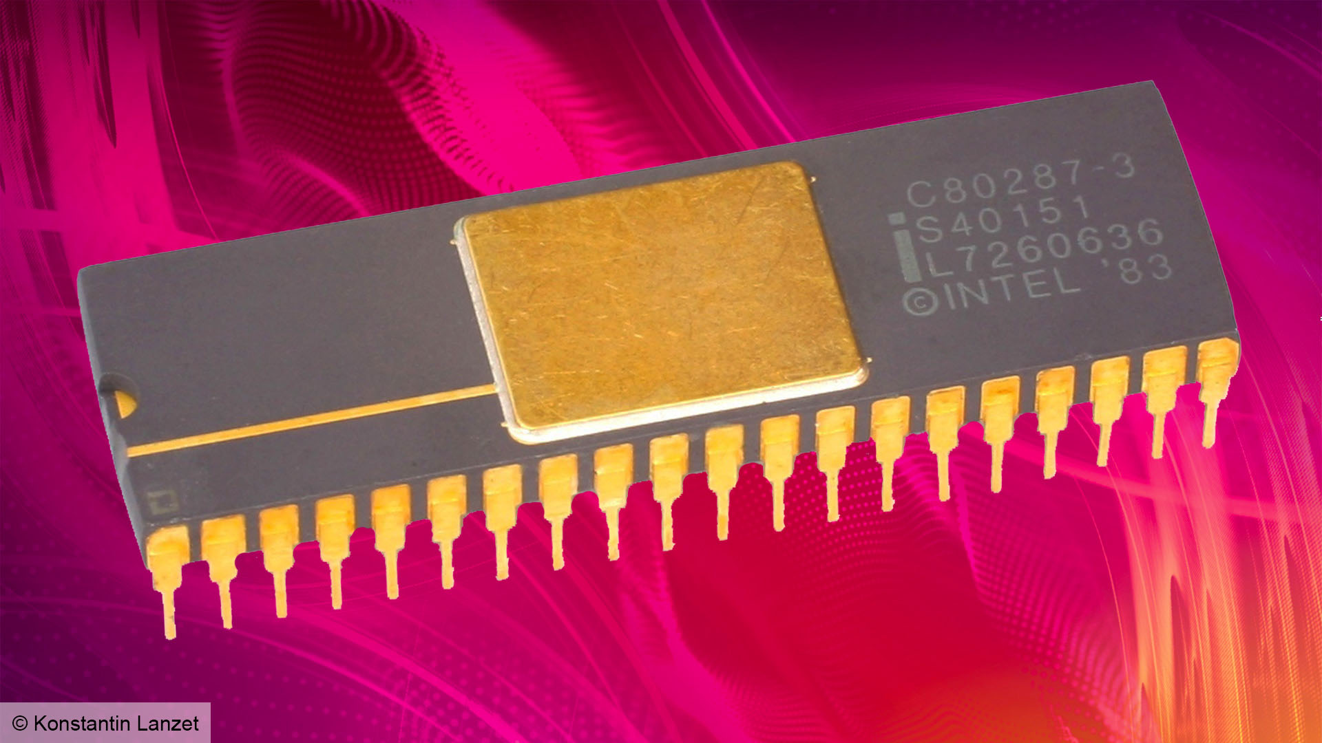
Since the 8086, floating-point coprocessor chips – popularly known as math coprocessors – had been made available as optional additions via a motherboard socket. They allowed addition, subtraction, multiplication, division, and square root calculations on numbers with decimal points to be carried out more quickly than on a standard integer unit, improving performance in arithmetic-intensive applications.
Originally, that was mostly accounting and computer-aided design (CAD) software, but later games were also able to take advantage of the hardware, notably including 1989’s SimCity and flight sims such as Falcon 3 in 1991. The 486SX series was the last range of Intel CPUs to be released without a built-in maths coprocessor – its sibling 486DX integrated a floating point unit into the CPU.

Intel 286 performance
The 286 provided a marked performance boost over the 8086 and 8088. This was in part down to faster clock speeds, particularly when 12.5MHz, 16MHz, and even faster 286 CPUs became popular. The CPU also benefited from significant architectural redesigns, enabling a 10MHz 286 to execute programs up to six times faster than a 5MHz 8086, according to Intel’s Introduction to the iAPX 286 document.
A 12MHz 286 can calculate between 1.28 and 2.66 million instructions per second (MIPS), compared to 0.330 MIPS for a 5MHz 8086 and 0.750 MIPS for a 10MHz 8088. The 286’s instructions per clock (IPC) count works out at 0.21 MIPS per megahertz.
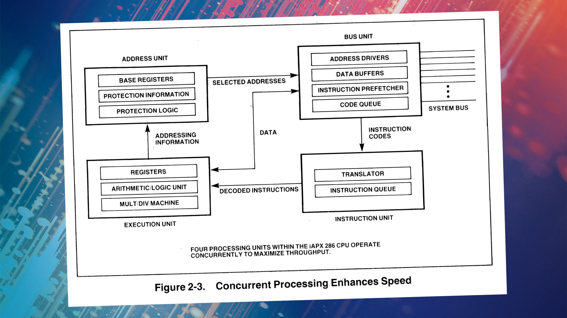
To help achieve this, the 80286 CPU comprises four independent processing units: address unit, bus unit, instruction unit, and execution unit, compared with the two-unit execution and bus organization of the 8086. It has demultiplexed address and data buses to improve bus efficiency, particularly in protected mode.
The instruction unit can decode and hold a queue of three prefetched instructions, which it sequentially feeds to the execution unit. Meanwhile, the presence of a dedicated address unit, which calculated the physical addresses in memory of the instruction and data being called upon, offered a key performance improvement over previous systems.

Intel 286 gaming
The 286’s extra power meant that more was possible for game developers. New instructions for moving data between stacks and registers benefited those working in high-level languages such as C. Although the increasing multimedia capabilities of PC systems through the 1980s also played a significant role, the PC’s processor power was becoming apparent. That said, in the 1980s, 286 systems were still prohibitively expensive compared with more family-orientated microcomputers, as well as low-end 8086-based PC-compatible machines.
Despite this, the second installment in Sierra’s King’s Quest series, 1985’s Romancing the Throne, explicitly supported the 286-based IBM PC/AT, booting directly from a floppy disk. By 1990, popular series, such as Ultima and Wizardry, which had once been developed for rival systems, such as the Apple II and IIGS, were receiving MS-DOS first releases.
It wasn’t all positive. Some older games whose performance was fixed to clock cycles became unplayably fast, which led to the widespread use of ‘Turbo buttons’, which would slow the system down to clock speeds comparable with 8086 and 8088 CPUs. Other 286 PCs had a BIOS option to do the same, and utilities such as Mo’Slo were developed in the 1990s to slow down overspeed games.
Today’s PC processors have moved on massively since the 1980s, but they’re still based on the same core x86 instruction set. If you’re looking to upgrade to one of the latest CPUs, make sure you read our full guide to the best gaming CPU, which covers the best options at a range of prices.
One of our current favorite chips from the company that developed the 286 – our old friend Intel – is the Core i5-13600K, which gives you loads of performance for the money, and you can read our full guide on how to overclock the Core i5-13600K as well.
We hope you’ve enjoyed this retrospective look at Intel’s 286 CPU. For more articles about the PC’s vintage history, check out our Retro tech page. If you’re old enough to remember the 286, take a look at our feature on CGA graphics.
